- 您现在的位置:买卖IC网 > PDF目录9191 > IDT72V8980J8 (IDT, Integrated Device Technology Inc)IC DGTL SW 256X256 44-PLCC PDF资料下载
参数资料
| 型号: | IDT72V8980J8 |
| 厂商: | IDT, Integrated Device Technology Inc |
| 文件页数: | 6/11页 |
| 文件大小: | 0K |
| 描述: | IC DGTL SW 256X256 44-PLCC |
| 标准包装: | 450 |
| 系列: | 72V |
| 类型: | 多路复用器 |
| 电路: | 1 x 8:8 |
| 独立电路: | 1 |
| 电压电源: | 单电源 |
| 电源电压: | 3 V ~ 3.6 V |
| 工作温度: | -40°C ~ 85°C |
| 安装类型: | 表面贴装 |
| 封装/外壳: | 44-LCC(J 形引线) |
| 供应商设备封装: | 44-PLCC(16.59x16.59) |
| 包装: | 带卷 (TR) |
| 其它名称: | 72V8980J8 |
4
Commercial Temperature Range
IDT72V8980 3.3V Time Slot Interchange
Digital Switch 256 x 256
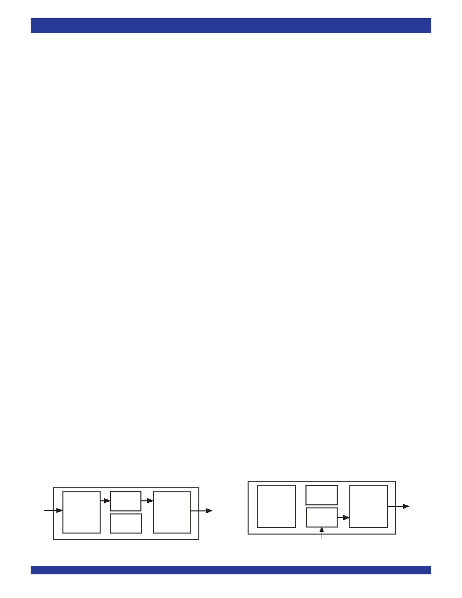
Data to be output on the serial streams may come from two sources: Data
Memory or Connection Memory. The Connection Memory is 16 bits wide and
is split into two 8-bit blocks—Connection Memory HIGH and Connection
Memory LOW. Each location in Connection Memory is associated with a
particularchannelintheoutputstreamsoastoprovideaone-to-onecorrespon-
dencebetweenthetwomemories. Thiscorrespondenceallowsforperchannel
control for each TX output stream. In Processor Mode, data output on the TX
stream is taken from the Connect Memory Low and originates from the
microprocessor (Figure 2). Where as in Connection Mode (Figure 1), data is
read from Data Memory using the address in Connection Memory. Data
destined for a particular channel on the serial output stream is read during the
previouschanneltimeslottoallowtimeformemoryaccessandinternalparallel-
to-serial conversion.
CONNECTION MODE
In Connection Mode, the addresses of input source for all output channels
are stored in the Connect Memory Low. The Connect Memory Low locations
are mapped to corresponding 8-bit x 32-channel output. The contents of the
Data Memory at the selected address are then transferred to the parallel-to-
serial converters. By having the output channel to specify the input channel
throughtheconnectmemory,inputchannelscanbebroadcasttoseveraloutput
channels.
PROCESSOR MODE
In Processor Mode the CPU writes data to specific Connect Memory Low
locationswhicharetobeoutputontheTXstreams. ThecontentsoftheConnect
Memory Low are transferred to the parallel-to-serial converter one channel
before it is to be output and are transmitted each frame to the output until it is
changed by the CPU.
CONTROL
The Connect Memory High bits (Table 4) control the per-channel functions
availableintheIDT72V8980.Outputchannelsareselectedintospecificmodes
such as: Processor Mode or Connection mode and Output Drivers Enabled
or in three-state condition. There is also one bit to control the state of the CCO
outputpin.
OUTPUT DRIVE ENABLE (ODE)
The ODE pin is the master output control pin. If the ODE input is held LOW
all TDM outputs will be placed in high impedance regardless Connect Memory
Highprogramming. However,ifODEisHIGH,thecontentsofConnectMemory
High control the output state on a per-channel basis.
DELAY THROUGH THE IDT72V8980
The transfer of information from the input serial streams to the output serial
streamsresultsinadelaythroughthedevice.ThedelaythroughtheIDT72V8980
devicevariesaccordingtothecombinationofinputandoutputstreamsandthe
movementwithinthestreamfromchanneltochannel. Datareceivedonaninput
stream must first be stored in Data Memory before it is sent out.
As information enters the IDT72V8980 it must first pass through an internal
serial-to-parallel converter. Likewise, before data leaves the device, it must
passthroughtheinternalparallel-to-serialconverter. Thisdatapreparationhas
an effect on the channel positioning in the frame immediately following the
incomingframe—mainly,datacannotleaveinthesametimeslot,oninthetime
slotimmediatelyfollowing. Therefore,informationthatistobeoutputinthesame
channel position as the information is input, relative to the frame pulse, will be
output in the following frame. As well, information switched to the channel
immediately following the input channel will not be output in the time slot
immediatelyfollowingbutinthenexttimeslotallocatedtotheoutputchannel,one
framelater.
Whether information can be output during a following timeslot after the
informationenteredtheIDT72V8980dependsonwhichRXstreamthechannel
information enters on and which TX stream the information leaves on. This
situation is caused by the order in which input stream information is placed into
Data Memory and the order in which stream information is queued for output.
Table1showstheallowableinput/outputstreamcombinationsfortheminimum
2 channel delay.
SOFTWARE CONTROL
If the A5 address line input is LOW then the IDT72V8980 Internal Control
Register is addressed. If A5 input line is high, then the remaining address input
linesareusedtoselectthe32possiblechannelsperinputoroutputstream. The
address input lines and the Stream Address bits (STA) of the Control register
give the user the capability of selecting all positions of IDT72V8980 Data and
Connection memories. The IDT72V8980 memory mapping is illustrated in
Table 2 and Figure 3.
The data in the control register consists of Memory Select and Stream
Addressbits,SplitMemoryandProcessorModebits.InSplitMemorymode(Bit
7 of the Control register) reads are from the Data Memory and writes are to the
Connect Memory as specified by the Memory Select Bits (Bits 4 and 3 of the
Control Register). The Memory Select bits allow the Connect Memory High or
LOW or the Data Memory to be chosen, and the Stream Address bits define
internal memory subsections corresponding to input or output streams.
The Processor Enable bit (bit 6) places EVERY output channel on every
outputstreaminProcessorMode;i.e.,thecontentsoftheConnectMemoryLOW
(CML, see Table 5) are output on the TX output streams once every frame
unless the ODE input pin is LOW. If PE bit is HIGH, then the IDT72V8980
behaves as if bits 2 (Channel Source) and 0 (Output Enable) of every Connect
MemoryHigh(CMH)locationsweresettoHIGH,regardlessoftheactualvalue.
If PE is LOW, then bit 2 and 0 of each Connect Memory High location operates
normally. In this case, if bit 2 of the CMH is HIGH, the associated TX output
channel is in Processor Mode. If bit 2 of the CMH is LOW, then the contents of
theCMLdefinethesourceinformation(streamandchannel)ofthetimeslotthat
is to be switched to an output.
Data
Memory
Connection
Memory
5705 drw06
TX
Microprocessor
Receive
Serial Data
Streams
Transmit
Serial Data
Streams
Receive
Serial Data
Streams
5705 drw05
RX
TX
Transmit
Serial Data
Streams
Data
Memory
Connection
Memory
Figure 2. Processor Mode
Figure 1. Connection Mode
FUNCTIONAL DESCRIPTION (Cont'd)
相关PDF资料 |
PDF描述 |
|---|---|
| IDT728985JG8 | IC DGTL SW 256X256 44-PLCC |
| VI-25X-MW | CONVERTER MOD DC/DC 5.2V 100W |
| VE-BWZ-MX-F1 | CONVERTER MOD DC/DC 2V 30W |
| X9401WS24Z-2.7 | IC XDCP QUAD 64-TAP 10K 24-SOIC |
| MPC92433AE | IC SYNTHESIZER LVPECL 48-LQFP |
相关代理商/技术参数 |
参数描述 |
|---|---|
| IDT72V8980JG | 功能描述:IC DGTL SWITCH ST-BUS 44-PLCC RoHS:是 类别:集成电路 (IC) >> 逻辑 - 信号开关,多路复用器,解码器 系列:72V 标准包装:48 系列:74VHC 类型:多路复用器 电路:4 x 2:1 独立电路:1 输出电流高,低:8mA,8mA 电压电源:单电源 电源电压:2 V ~ 5.5 V 工作温度:-40°C ~ 85°C 安装类型:表面贴装 封装/外壳:16-SOIC(0.154",3.90mm 宽) 供应商设备封装:16-SOIC 包装:管件 |
| IDT72V8980JG8 | 功能描述:IC DGTL SW 256X256 44-PLCC RoHS:是 类别:集成电路 (IC) >> 逻辑 - 信号开关,多路复用器,解码器 系列:72V 标准包装:48 系列:74VHC 类型:多路复用器 电路:4 x 2:1 独立电路:1 输出电流高,低:8mA,8mA 电压电源:单电源 电源电压:2 V ~ 5.5 V 工作温度:-40°C ~ 85°C 安装类型:表面贴装 封装/外壳:16-SOIC(0.154",3.90mm 宽) 供应商设备封装:16-SOIC 包装:管件 |
| IDT72V8980PV | 功能描述:IC DGTL SW 256X256 48-SSOP RoHS:否 类别:集成电路 (IC) >> 逻辑 - 信号开关,多路复用器,解码器 系列:72V 标准包装:48 系列:74VHC 类型:多路复用器 电路:4 x 2:1 独立电路:1 输出电流高,低:8mA,8mA 电压电源:单电源 电源电压:2 V ~ 5.5 V 工作温度:-40°C ~ 85°C 安装类型:表面贴装 封装/外壳:16-SOIC(0.154",3.90mm 宽) 供应商设备封装:16-SOIC 包装:管件 |
| IDT72V8980PV8 | 功能描述:IC DGTL SW 256X256 48-SSOP RoHS:否 类别:集成电路 (IC) >> 逻辑 - 信号开关,多路复用器,解码器 系列:72V 标准包装:48 系列:74VHC 类型:多路复用器 电路:4 x 2:1 独立电路:1 输出电流高,低:8mA,8mA 电压电源:单电源 电源电压:2 V ~ 5.5 V 工作温度:-40°C ~ 85°C 安装类型:表面贴装 封装/外壳:16-SOIC(0.154",3.90mm 宽) 供应商设备封装:16-SOIC 包装:管件 |
| IDT72V8980PVG | 功能描述:IC DGTL SW 256X256 48-SSOP RoHS:是 类别:集成电路 (IC) >> 逻辑 - 信号开关,多路复用器,解码器 系列:72V 标准包装:48 系列:74VHC 类型:多路复用器 电路:4 x 2:1 独立电路:1 输出电流高,低:8mA,8mA 电压电源:单电源 电源电压:2 V ~ 5.5 V 工作温度:-40°C ~ 85°C 安装类型:表面贴装 封装/外壳:16-SOIC(0.154",3.90mm 宽) 供应商设备封装:16-SOIC 包装:管件 |
发布紧急采购,3分钟左右您将得到回复。