- 您现在的位置:买卖IC网 > PDF目录9191 > IDT72V8981J8 (IDT, Integrated Device Technology Inc)IC DGTL SW 128X128 44-PLCC PDF资料下载
参数资料
| 型号: | IDT72V8981J8 |
| 厂商: | IDT, Integrated Device Technology Inc |
| 文件页数: | 5/9页 |
| 文件大小: | 0K |
| 描述: | IC DGTL SW 128X128 44-PLCC |
| 标准包装: | 450 |
| 系列: | 72V |
| 类型: | 多路复用器 |
| 电路: | 1 x 4:4 |
| 独立电路: | 1 |
| 电压电源: | 单电源 |
| 电源电压: | 3 V ~ 3.6 V |
| 工作温度: | -40°C ~ 85°C |
| 安装类型: | 表面贴装 |
| 封装/外壳: | 44-LCC(J 形引线) |
| 供应商设备封装: | 44-PLCC(16.59x16.59) |
| 包装: | 带卷 (TR) |
| 其它名称: | 72V8981J8 |
5
Commercial Temperature Range
IDT72V8981 3.3V Time Slot Interchange
Digital Switch 128 x 128
INITIALIZATION OF THE IDT72V8981
On initialization or power up, the contents of the Connection Memory High
can be in any state. This is a potentially hazardous condition when multiple TX
outputs are tied together to form matrices. The ODE pin should be held low on
power up to keep all outputs in the high impedance condition until the contents
of the CMH are programmed.
TABLE 1 — INPUT STREAM TO OUT-
PUT STREAM COMBINATIONS THAT
CAN
PROVIDE
THE
MINIMUM
2-CHANNEL DELAY
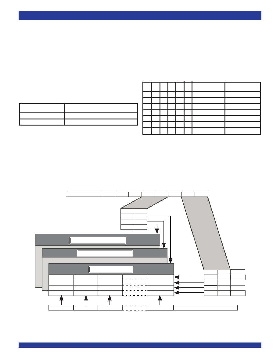
TABLE 2 — ADDRESS MAPPING
Connection Memory High
Channel 0
Channel 1
Channel 2
Channel 31
Channel 0
Channel 1
Channel 2
Channel 31
Channel 0
Channel 1
Channel 2
Channel 31
Channel 0
Channel 1
10000
1
10001
0
11111
1
Data Memory
0
1
0
2
1
3
0
1
0
1
10000
0
Channel 2
Channel 31
Connection Memory Low
Stream
Control Register
CRb7
External Address Bits
A5-A0
5702 drw07
The Control Register is only accessed when A5=0.
All other address bits have no effect when A5=0.
When A5 =1, only 32 bytes are randomly accessable
via A0-A4 at any one instant. Which 32 bytes are
accessed is determined by the state of CRb0 -CRb4.
The 32 bytes correlate to 32 channel of one ST-BUS
stream.
CRb6CRb5CRb4CRb3CRb2CRb1CRb0
CRb1CRb0
CRb4CRb3
Figure 3. Address Mapping
NOTES:
1. Writing to the Control Register is the only fast transaction.
2. Memory and stream are specified by the contents of the Control Register.
A5 A4 A3 A2 A1 A0
HEX ADDRESS
LOCATION
0
X
0
00-1F
Control Register(1)
100000
20
Channel 0(2)
100001
21
Channel 1(2)
1
1
1
111111
3F
Channel 31(2)
Input
Output Stream
0
1,2,3
13
Duringthemicroprocessorinitializationroutine,themicroprocessorshould
programthedesiredactivepathsthroughthematrices,andputallotherchannels
into the high impedance state. Care should be taken that no two connected TX
outputsdrivethebussimultaneously. WiththeCMHsetup,themicroprocessor
controlling the matrices can bring the ODE signal high to relinquish high
impedance state control to the Connection Memory High bits outputs.
相关PDF资料 |
PDF描述 |
|---|---|
| ICS844071AGLF | IC CLK GEN SAS LVDS 8-TSSOP |
| VE-BWZ-MY-F4 | CONVERTER MOD DC/DC 2V 20W |
| X9251UV24IZ-2.7T1 | IC XDCP QUAD 256TP 50K 24-TSSOP |
| VE-BWZ-MY-F2 | CONVERTER MOD DC/DC 2V 20W |
| IDT728981J | IC DGTL SW 256X256 44-PLCC |
相关代理商/技术参数 |
参数描述 |
|---|---|
| IDT72V8981JG | 功能描述:IC DGTL SW 128X128 44-PLCC RoHS:是 类别:集成电路 (IC) >> 逻辑 - 信号开关,多路复用器,解码器 系列:72V 标准包装:48 系列:74VHC 类型:多路复用器 电路:4 x 2:1 独立电路:1 输出电流高,低:8mA,8mA 电压电源:单电源 电源电压:2 V ~ 5.5 V 工作温度:-40°C ~ 85°C 安装类型:表面贴装 封装/外壳:16-SOIC(0.154",3.90mm 宽) 供应商设备封装:16-SOIC 包装:管件 |
| IDT72V8981JG8 | 功能描述:IC DGTL SW 128X128 44-PLCC RoHS:是 类别:集成电路 (IC) >> 逻辑 - 信号开关,多路复用器,解码器 系列:72V 标准包装:48 系列:74VHC 类型:多路复用器 电路:4 x 2:1 独立电路:1 输出电流高,低:8mA,8mA 电压电源:单电源 电源电压:2 V ~ 5.5 V 工作温度:-40°C ~ 85°C 安装类型:表面贴装 封装/外壳:16-SOIC(0.154",3.90mm 宽) 供应商设备封装:16-SOIC 包装:管件 |
| IDT72V8985J | 功能描述:IC DGTL SW 256X256 44-PLCC RoHS:否 类别:集成电路 (IC) >> 逻辑 - 信号开关,多路复用器,解码器 系列:72V 标准包装:48 系列:74VHC 类型:多路复用器 电路:4 x 2:1 独立电路:1 输出电流高,低:8mA,8mA 电压电源:单电源 电源电压:2 V ~ 5.5 V 工作温度:-40°C ~ 85°C 安装类型:表面贴装 封装/外壳:16-SOIC(0.154",3.90mm 宽) 供应商设备封装:16-SOIC 包装:管件 |
| IDT72V8985J8 | 功能描述:IC DGTL SW 256X256 44-PLCC RoHS:否 类别:集成电路 (IC) >> 逻辑 - 信号开关,多路复用器,解码器 系列:72V 标准包装:48 系列:74VHC 类型:多路复用器 电路:4 x 2:1 独立电路:1 输出电流高,低:8mA,8mA 电压电源:单电源 电源电压:2 V ~ 5.5 V 工作温度:-40°C ~ 85°C 安装类型:表面贴装 封装/外壳:16-SOIC(0.154",3.90mm 宽) 供应商设备封装:16-SOIC 包装:管件 |
| IDT72V8985JG | 功能描述:IC DGTL SW ST-BUS/GCI 44-PLCC RoHS:是 类别:集成电路 (IC) >> 逻辑 - 信号开关,多路复用器,解码器 系列:72V 标准包装:48 系列:74VHC 类型:多路复用器 电路:4 x 2:1 独立电路:1 输出电流高,低:8mA,8mA 电压电源:单电源 电源电压:2 V ~ 5.5 V 工作温度:-40°C ~ 85°C 安装类型:表面贴装 封装/外壳:16-SOIC(0.154",3.90mm 宽) 供应商设备封装:16-SOIC 包装:管件 |
发布紧急采购,3分钟左右您将得到回复。