- 您现在的位置:买卖IC网 > PDF目录9187 > IDT72V90823J (IDT, Integrated Device Technology Inc)IC DGTL SW 2048X2048 84-PLCC PDF资料下载
参数资料
| 型号: | IDT72V90823J |
| 厂商: | IDT, Integrated Device Technology Inc |
| 文件页数: | 16/21页 |
| 文件大小: | 0K |
| 描述: | IC DGTL SW 2048X2048 84-PLCC |
| 标准包装: | 30 |
| 系列: | 72V |
| 类型: | 多路复用器 |
| 电路: | 1 x 16:16 |
| 独立电路: | 1 |
| 电压电源: | 单电源 |
| 电源电压: | 3 V ~ 3.6 V |
| 工作温度: | -40°C ~ 85°C |
| 安装类型: | 表面贴装 |
| 封装/外壳: | 84-LCC(J 形引线) |
| 供应商设备封装: | 84-PLCC(29.21x29.21) |
| 包装: | 管件 |
| 其它名称: | 72V90823J |
4
IDT72V90823A 3.3V TIME SLOT INTERCHANGE
DIGITAL SWITCH 2,048 x 2,048
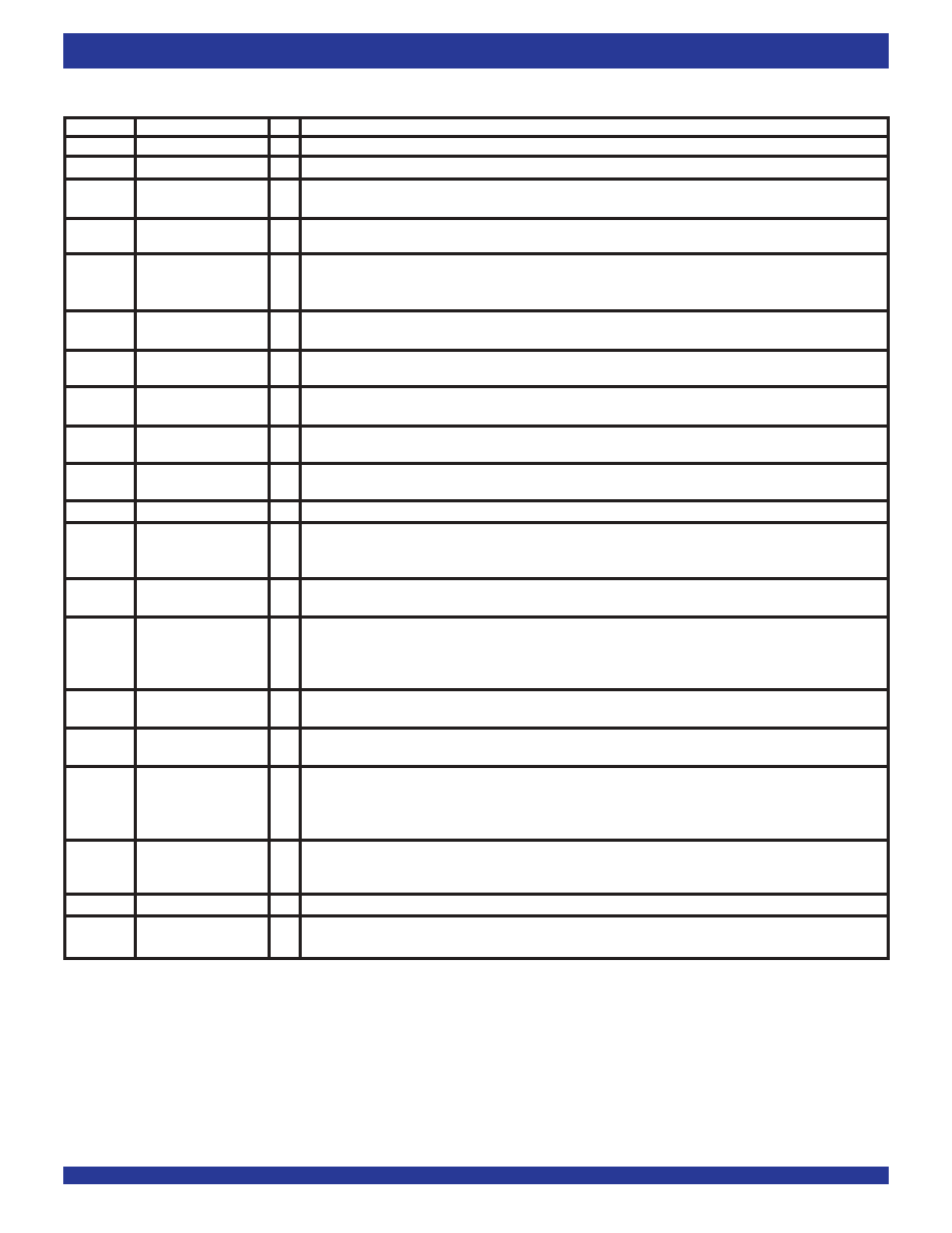
PIN DESCRIPTION
SYMBOL
NAME
I/O
DESCRIPTION
GND
Ground.
Ground Rail.
Vcc
+3.3 Volt Power Supply.
TX0-15(1)
TX Output 0 to 15
O
Serial data output stream. These streams may have data rates of 2.048, 4.096 or 8.192 Mb/s, depending upon
(Three-state Outputs)
the value programmed at bits DR0-1 in the IMS register.
RX0-15(1)
RX Input 0 to 15
I
Serial data input stream. These streams may have data rates of 2.048, 4.096 or 8.192 Mb/s, depending upon
the value programmed at bits DR0-1 in the IMS register.
F0i(1)
Frame Pulse
I
When the WFPS pin is LOW, this input accepts and automatically identifies frame synchronization signals formatted
according to ST-BUS and GCI specifications. When the WFPS pin is HIGH, this pin accepts a negative frame
pulse which conforms to WFPS formats.
FE/HCLK(1) Frame Evaluation/
I
When the WFPS pin is LOW, this pin is the frame measurement input. When the WFPS pin is HIGH, the HCLK
HCLK Clock
(4.096 MHz clock) is required for frame alignment in the wide frame pulse (WFP) mode.
CLK(1)
Clock
I
Serial clock for shifting data in/out on the serial streams (RX/TX 0-15). Depending upon the value programmed
at bits DR0-1 in the IMS register, this input accepts a 4.096, 8.192 or 16.384 MHz clock.
TMS
Test Mode Select
I
JTAG signal that controls the state transitions of the TAP controller. This pin is pulled HIGH by an internal pull-
up when not driven.
TDI
Test Serial Data In
I
JTAG serial test instructions and data are shifted in on this pin. This pin is pulled HIGH by an internal pull-up
when not driven.
TDO
Test Serial Data Out
O
JTAG serial data is output on this pin on the falling edge of TCK. This pin is held in high-impedance state when
JTAG scan is not enabled.
TCK(1)
Test Clock
I
Provides the clock to the JTAG test logic.
TRST
Test Reset
I
Asynchronously initializes the JTAG TAP controller by putting it in the Test-Logic-reset state. This pin is pulled
by an internal pull-up when not driven. This pin should be pulsed LOW on power-up, or held LOW, to ensure
that the IDT72V90823 is in the normal functional mode.
IC(1)
Internal Connection
I
Connect to GND for normal operation. This pin must be low for the IDT72V90823 to function normally and to comply
with IEEE 1114 (JTAG) boundary scan requirements.
RESET(1)
Device Reset
I
This input (active LOW) puts the IDT72V90823 in its reset state that clears the device internal counters, registers
(Schmitt Trigger Input)
and brings TX0-15 and microport data outputs to a high-impedance state. The time constant for a power up
reset circuit must be a minimum of five times the rise time of the power supply. In normal operation, the
RESET
pin must be held LOW for a minimum of 100ns to reset the device.
WFPS(1)
Wide Frame
I
When 1, enables the wide frame pulse (WFP) Frame Alignment interface. When 0, the device operates in
Pulse Select
ST-BUS/GCI mode.
A0-7(1)
Address 0-7
I
When non-multiplexed CPU bus operation is selected, these lines provide the A0-A7 address lines to the internal
memories.
DS/
RD(1)
Data Strobe/Read
I
For Motorola multiplexed bus operation, this input is DS. This active HIGH DS input works in conjunction with
CS
to enable the read and write operations. For Motorola non-multiplexed CPU bus operation, this input is DS. This
active LOW input works in conjunction with
CS to enable the read and write operations. For Intel multiplexed bus
operation, this input is
RD. This active LOW input sets the data bus lines (AD0-7, D8-15) as outputs.
R/
W / WR(1) Read/Write / Write
I
In the cases of Motorola non-multiplexed and multiplexed bus operations, this input is R/
W. This input controls
the direction of the data bus lines (AD0-7, D8-15) during a microprocessor access. For Intel multiplexed bus
operation, this input is
WR. This active LOW input is used with RD to control the data bus (AD0-7) lines as inputs.
CS(1)
Chip Select
I
Active LOW input used by a microprocessor to activate the microprocessor port of IDT72V90823.
AS/ALE(1)
Address Strobe or
I
This input is used if multiplexed bus operation is selected via the IM input pin. For Motorola non-multiplexed
Latch Enable
bus operation, connect this pin to ground.
NOTE:
1. These pins are 5V tolerant.
相关PDF资料 |
PDF描述 |
|---|---|
| IDT7290820JG | IC DGTL SW 2048X2048 84-PLCC |
| MAX5527GUA+T | IC POT DGTL 1TIME PROGR 8-UMAX |
| IDT7290820J | IC DGTL SW 2048X2048 84-PLCC |
| VI-BWW-MY-F2 | CONVERTER MOD DC/DC 5.5V 50W |
| VI-BWW-MY-F1 | CONVERTER MOD DC/DC 5.5V 50W |
相关代理商/技术参数 |
参数描述 |
|---|---|
| IDT72V90823J8 | 功能描述:IC DGTL SW 2048X2048 84-PLCC RoHS:否 类别:集成电路 (IC) >> 逻辑 - 信号开关,多路复用器,解码器 系列:72V 标准包装:48 系列:74VHC 类型:多路复用器 电路:4 x 2:1 独立电路:1 输出电流高,低:8mA,8mA 电压电源:单电源 电源电压:2 V ~ 5.5 V 工作温度:-40°C ~ 85°C 安装类型:表面贴装 封装/外壳:16-SOIC(0.154",3.90mm 宽) 供应商设备封装:16-SOIC 包装:管件 |
| IDT72V90823JG | 功能描述:IC DGTL SW 2048X2048 84-PLCC RoHS:是 类别:集成电路 (IC) >> 逻辑 - 信号开关,多路复用器,解码器 系列:72V 标准包装:48 系列:74VHC 类型:多路复用器 电路:4 x 2:1 独立电路:1 输出电流高,低:8mA,8mA 电压电源:单电源 电源电压:2 V ~ 5.5 V 工作温度:-40°C ~ 85°C 安装类型:表面贴装 封装/外壳:16-SOIC(0.154",3.90mm 宽) 供应商设备封装:16-SOIC 包装:管件 |
| IDT72V90823JG8 | 功能描述:IC DGTL SW 2048X2048 84-PLCC RoHS:是 类别:集成电路 (IC) >> 逻辑 - 信号开关,多路复用器,解码器 系列:72V 标准包装:48 系列:74VHC 类型:多路复用器 电路:4 x 2:1 独立电路:1 输出电流高,低:8mA,8mA 电压电源:单电源 电源电压:2 V ~ 5.5 V 工作温度:-40°C ~ 85°C 安装类型:表面贴装 封装/外壳:16-SOIC(0.154",3.90mm 宽) 供应商设备封装:16-SOIC 包装:管件 |
| IDT72V90823PF | 功能描述:IC DGTL SW 2048X2048 100-TQFP RoHS:否 类别:集成电路 (IC) >> 逻辑 - 信号开关,多路复用器,解码器 系列:72V 标准包装:48 系列:74VHC 类型:多路复用器 电路:4 x 2:1 独立电路:1 输出电流高,低:8mA,8mA 电压电源:单电源 电源电压:2 V ~ 5.5 V 工作温度:-40°C ~ 85°C 安装类型:表面贴装 封装/外壳:16-SOIC(0.154",3.90mm 宽) 供应商设备封装:16-SOIC 包装:管件 |
| IDT72V90823PF8 | 功能描述:IC DGTL SW 2048X2048 100-TQFP RoHS:否 类别:集成电路 (IC) >> 逻辑 - 信号开关,多路复用器,解码器 系列:72V 标准包装:48 系列:74VHC 类型:多路复用器 电路:4 x 2:1 独立电路:1 输出电流高,低:8mA,8mA 电压电源:单电源 电源电压:2 V ~ 5.5 V 工作温度:-40°C ~ 85°C 安装类型:表面贴装 封装/外壳:16-SOIC(0.154",3.90mm 宽) 供应商设备封装:16-SOIC 包装:管件 |
发布紧急采购,3分钟左右您将得到回复。