- 您现在的位置:买卖IC网 > PDF目录67115 > IDT74ALVCH16260PAG8 (INTEGRATED DEVICE TECHNOLOGY INC) ALVC/VCX/A SERIES, 12 1 LINE TO 2 LINE MULTIPLEXER AND DEMUX/DECODER, TRUE OUTPUT, PDSO56 PDF资料下载
参数资料
| 型号: | IDT74ALVCH16260PAG8 |
| 厂商: | INTEGRATED DEVICE TECHNOLOGY INC |
| 元件分类: | 编、解码器及复用、解复用 |
| 英文描述: | ALVC/VCX/A SERIES, 12 1 LINE TO 2 LINE MULTIPLEXER AND DEMUX/DECODER, TRUE OUTPUT, PDSO56 |
| 封装: | GREEN, TSSOP-56 |
| 文件页数: | 1/7页 |
| 文件大小: | 82K |
| 代理商: | IDT74ALVCH16260PAG8 |
INDUSTRIALTEMPERATURERANGE
IDT74ALVCH16260
3.3V CMOS 12-BIT TO 24-BIT MULTIPLEXED D-TYPE LATCH
1
MARCH 2006
INDUSTRIAL TEMPERATURE RANGE
The IDT logo is a registered trademark of Integrated Device Technology, Inc.
2006 Integrated Device Technology, Inc.
DSC-4737/5
FEATURES:
0.5 MICRON CMOS Technology
Typical tSK(o) (Output Skew) < 250ps
ESD > 2000V per MIL-STD-883, Method 3015; > 200V using
machine model (C = 200pF, R = 0)
VCC = 3.3V ± 0.3V, Normal Range
VCC = 2.7V to 3.6V, Extended Range
VCC = 2.5V ± 0.2V
CMOS power levels (0.4
μμμμμ W typ. static)
Rail-to-Rail output swing for increased noise margin
Available in TSSOP package
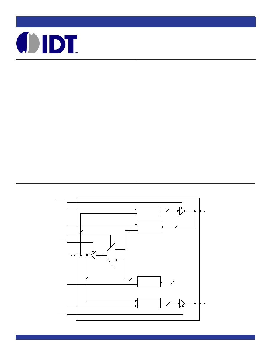
FUNCTIONAL BLOCK DIAGRAM
IDT74ALVCH16260
3.3V CMOS 12-BIT TO 24-BIT
MULTIPLEXED D-TYPE LATCH
WITH 3-STATE OUTPUTS
AND BUS-HOLD
DESCRIPTION:
This 12-bit to 24-bit multiplexed D-type latch is built using advanced dual
metal CMOS technology. The ALVCH16260 is used in applications in which
two separate data paths must be multiplexed onto, or demultiplexed from, a
singledatapath.Typicalapplicationsincludemultiplexingand/ordemultiplexing
addressanddatainformationinmicroprocessororbus-interfaceapplications.
This device also is useful in memory interleaving applications.
Three 12-bit I/O ports (A1-A12, 1B1-1B12, and 2B1-2B12) are available
foraddressand/ordatatransfer.Theoutput-enable(
OE1B,OE2B,andOEA)
inputs control the bus transceiver functions. The
OE1B and OE2B control
signals also allow bank control in the A-to-B direction. Address and/or data
informationcanbestoredusingtheinternalstoragelatches.Thelatch-enable
(LE1B, LE2B, LEA1B, and LEA2B) inputs are used to control data storage.
When the latch-enable input is high, the latch is transparent. When the latch-
enable input goes low, the data present at the inputs is latched and remains
latched until the latch-enable input is returned high.
The ALVCH16260 has been designed with a ±24mA output driver. This
driver is capable of driving a moderate to heavy load while maintaining speed
performance.
The ALVCH16260 has “bus-hold” which retains the inputs’ last state
whenever the input goes to a high impedance. This prevents floating inputs
and eliminates the need for pull-up/down resistors.
APPLICATIONS:
3.3V high speed systems
3.3V and lower voltage computing systems
DRIVE FEATURES:
High Output Drivers: ±24mA
Suitable for heavy loads
LE1B
LEA1B
OE1B
SEL
OEA
A1:12
LE2B
LEA2B
OE2B
A-1B
LATCH
1B-A
LATCH
A-2B
LATCH
2B-A
LATCH
M
U
X
1
0
12
1
B1:12
2
B1:12
12
30
29
2
28
1
27
55
56
相关PDF资料 |
PDF描述 |
|---|---|
| IDT74ALVCH16276PF | ALVC/VCX/A SERIES, 12-BIT EXCHANGER, TRUE OUTPUT, PDSO56 |
| IDT74ALVCH16276PVG | ALVC/VCX/A SERIES, 12-BIT EXCHANGER, TRUE OUTPUT, PDSO56 |
| IDT74ALVCH16276PV8 | ALVC/VCX/A SERIES, 12-BIT EXCHANGER, TRUE OUTPUT, PDSO56 |
| IDT74ALVCH162827PF | ALVC/VCX/A SERIES, DUAL 10-BIT DRIVER, TRUE OUTPUT, PDSO56 |
| IDT74ALVCH162827PV8 | ALVC/VCX/A SERIES, DUAL 10-BIT DRIVER, TRUE OUTPUT, PDSO56 |
相关代理商/技术参数 |
参数描述 |
|---|---|
| IDT74ALVCH162820PAG | 功能描述:IC FLIP FLOP 3ST 10BIT 56TSSOP RoHS:是 类别:集成电路 (IC) >> 逻辑 - 触发器 系列:74ALVCH 标准包装:1 系列:74LVX 功能:主复位 类型:D 型总线 输出类型:非反相 元件数:1 每个元件的位元数:8 频率 - 时钟:150MHz 延迟时间 - 传输:7.1ns 触发器类型:正边沿 输出电流高,低:4mA,4mA 电源电压:2 V ~ 3.6 V 工作温度:-40°C ~ 85°C 安装类型:表面贴装 封装/外壳:20-TSSOP(0.173",4.40mm 宽) 包装:Digi-Reel® 其它名称:74LVX273MTCXDKR |
| IDT74ALVCH162820PAG8 | 功能描述:IC FLIP FLOP 3ST 10BIT 56TSSOP RoHS:是 类别:集成电路 (IC) >> 逻辑 - 触发器 系列:74ALVCH 标准包装:1 系列:74LVX 功能:主复位 类型:D 型总线 输出类型:非反相 元件数:1 每个元件的位元数:8 频率 - 时钟:150MHz 延迟时间 - 传输:7.1ns 触发器类型:正边沿 输出电流高,低:4mA,4mA 电源电压:2 V ~ 3.6 V 工作温度:-40°C ~ 85°C 安装类型:表面贴装 封装/外壳:20-TSSOP(0.173",4.40mm 宽) 包装:Digi-Reel® 其它名称:74LVX273MTCXDKR |
| IDT74ALVCH162825APF | 制造商:Rochester Electronics LLC 功能描述:- Bulk |
| IDT74ALVCH16501PA | 制造商:Integrated Device Technology Inc 功能描述:Bus Transceiver, Single, 18 Bit, 56 Pin, Plastic, TSSOP |
| IDT74ALVCH16501PAG | 功能描述:IC UNIV BUS TXRX 18BIT 56TSSOP RoHS:是 类别:集成电路 (IC) >> 逻辑 - 通用总线函数 系列:74ALVCH 产品变化通告:Product Discontinuation 09/Dec/2010 标准包装:1,500 系列:74AVC 逻辑类型:通用总线驱动器 输入数:- 电路数:18 位 输出电流高,低:12mA,12mA 电源电压:1.65 V ~ 3.6 V 工作温度:-40°C ~ 85°C 安装类型:表面贴装 封装/外壳:56-TFSOP(0.240",6.10mm 宽) 供应商设备封装:56-TSSOP 包装:带卷 (TR) |
发布紧急采购,3分钟左右您将得到回复。