- 您现在的位置:买卖IC网 > PDF目录65581 > IDT74FCT139TDC (INTEGRATED DEVICE TECHNOLOGY INC) FCT SERIES, OTHER DECODER/DRIVER, INVERTED OUTPUT, PDSO16 PDF资料下载
参数资料
| 型号: | IDT74FCT139TDC |
| 厂商: | INTEGRATED DEVICE TECHNOLOGY INC |
| 元件分类: | 编、解码器及复用、解复用 |
| 英文描述: | FCT SERIES, OTHER DECODER/DRIVER, INVERTED OUTPUT, PDSO16 |
| 封装: | 0.150 INCH, SOIC-16 |
| 文件页数: | 4/6页 |
| 文件大小: | 141K |
| 代理商: | IDT74FCT139TDC |
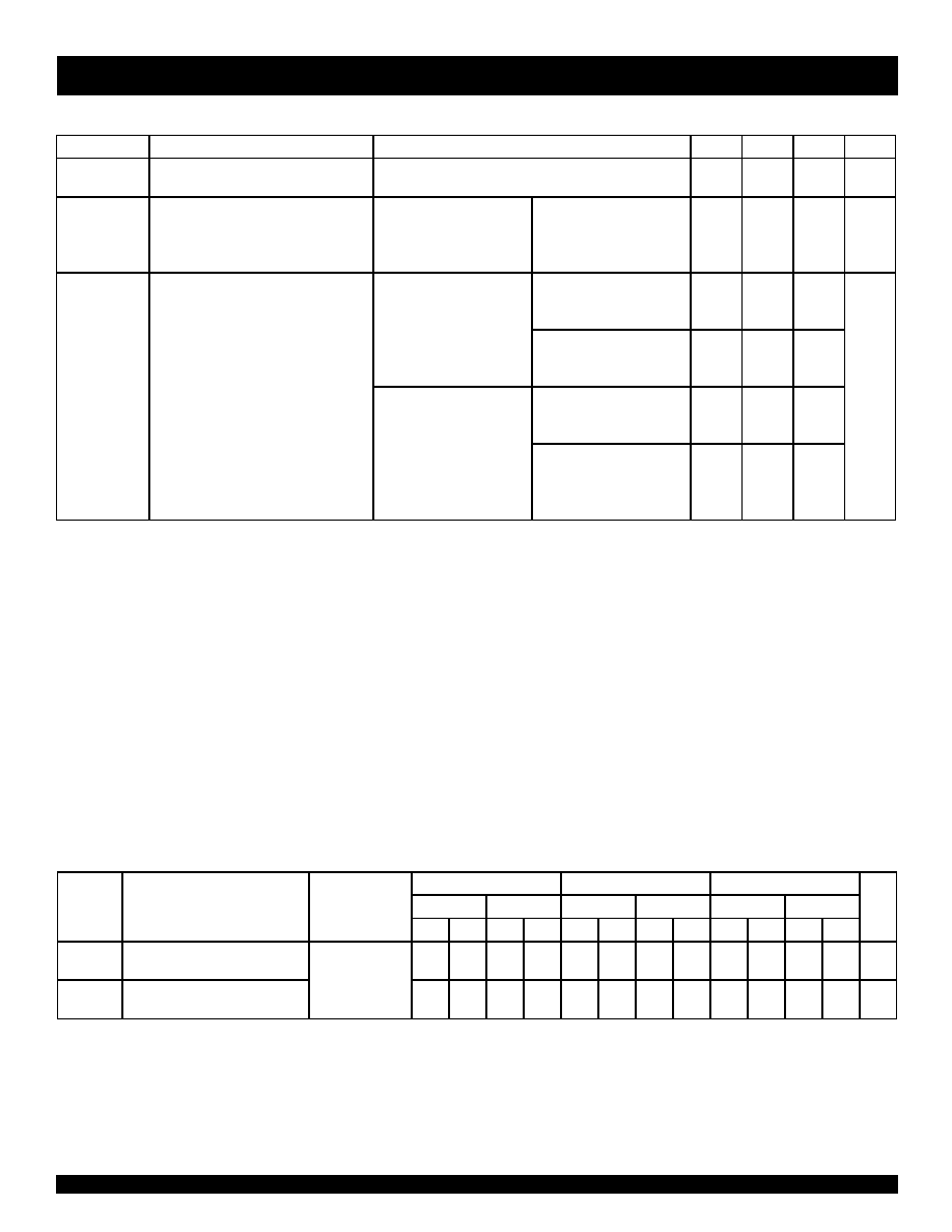
4
MILITARYANDINDUSTRIALTEMPERATURERANGE
IDT54/74FCT139T/AT/CT
FAST CMOS DUAL 1-OF-4 DECODER WITH ENABLE
POWER SUPPLY CHARACTERISTICS
Symbol
Parameter
Test Conditions(1)
Min.
Typ.(2)
Max.
Unit
ICC
Quiescent Power Supply Current
TTL Inputs HIGH
VCC = Max.
VIN = 3.4V(3)
—0.5
2
mA
ICCD
Dynamic Power Supply Current(4)
VCC = Max.
Outputs Open
One Bit Toggling
50% Duty Cycle
VIN = VCC
VIN = GND
—
0.15
0.3
mA/
MHz
IC
Total Power Supply Current(6)
VCC = Max.
Outputs Open
fo = 10MHz
VIN = VCC
VIN = GND
—1.5
4
mA
50% Duty Cycle
One Input and
One Output Toggling
VIN = 3.4V
VIN = GND
—1.8
5
VCC = Max.
Outputs Open
fo = 10MHz
VIN = VCC
VIN = GND
—3
7(5)
50% Duty Cycle
One Input Toggling
on Each Decoder
Two Outputs Toggling
VIN = 3.4V
VIN = GND
—3.5
9(5)
NOTES:
1. For conditions shown as Max. or Min., use appropriate value specified under Electrical Characteristics for the applicable device type.
2. Typical values are at VCC = 5.0V, +25°C ambient.
3. Per TTL driven input (VIN = 3.4V). All other inputs at VCC or GND.
4. This parameter is not directly testable, but is derived for use in Total Power Supply Calculations.
5. Values for these conditions are examples of the ICC formula. These limits are guaranteed but not tested.
6. IC = IQUIESCENT + IINPUTS + IDYNAMIC
IC = ICC +
ICC DHNT + ICCD (fONO)
ICC = Quiescent Current
ICC = Power Supply Current for a TTL High Input (VIN = 3.4V)
DH = Duty Cycle for TTL Inputs High
NT = Number of TTL Inputs at DH
ICCD = Dynamic Current Caused by an Input Transition Pair (HLH or LHL)
fO = Output Frequency
NO = Number of Outputs at fO
All currents are in milliamps and all frequencies are in megahertz.
SWITCHING CHARACTERISTICS OVER OPERATING RANGE
FCT139T
FCT139AT
FCT139CT
Ind.
Mil.
Ind.
Mil.
Ind.
Mil.
Parameter
Description
Condition(1)
Min. (2) Max. Min. (2) Max. Min. (2) Max. Min. (2) Max. Min. (2) Max. Min. (2) Max.
Unit
tPLH
tPHL
Propagation Delay
A0 or A1 to
On
CL = 50pF
RL = 500
1.5
9
1.5
12
1.5
5.9
1.5
7.8
1.5
5
1.5
6.2
ns
tPLH
tPHL
Propagation Delay
E to On
1.5
8
1.5
9
1.5
5.5
1.5
7.2
1.5
4.8
1.5
5.8
ns
NOTES:
1. See test circuit and waveforms.
2. Minimum limits are guaranteed but not tested on Propagation Delays.
相关PDF资料 |
PDF描述 |
|---|---|
| IDT74FCT151CTSO8 | FCT SERIES, 8 LINE TO 1 LINE MULTIPLEXER, COMPLEMENTARY OUTPUT, PDSO16 |
| IDT74FCT157DTLG | FCT SERIES, QUAD 2 LINE TO 1 LINE MULTIPLEXER, TRUE OUTPUT, CQCC20 |
| IDT74FCT158CTDCG | FCT SERIES, QUAD 2 LINE TO 1 LINE MULTIPLEXER, TRUE OUTPUT, PDSO16 |
| IDT74FCT158CTDC | FCT SERIES, QUAD 2 LINE TO 1 LINE MULTIPLEXER, TRUE OUTPUT, PDSO16 |
| IDT74FCT158ATDC | FCT SERIES, QUAD 2 LINE TO 1 LINE MULTIPLEXER, TRUE OUTPUT, PDSO16 |
相关代理商/技术参数 |
参数描述 |
|---|---|
| IDT74FCT139TQ | 制造商:Rochester Electronics LLC 功能描述:- Bulk |
| IDT74FCT151ATSO | 制造商:Integrated Device Technology Inc 功能描述: |
| IDT74FCT151KATP | 制造商:Integrated Device Technology Inc 功能描述: |
| IDT74FCT151TSO | 制造商:Integrated Device Technology Inc 功能描述: |
| IDT74FCT157ATQ | 制造商:Integrated Device Technology Inc 功能描述: |
发布紧急采购,3分钟左右您将得到回复。