- 您现在的位置:买卖IC网 > PDF目录65586 > IDT74FCT273ATQ8 (INTEGRATED DEVICE TECHNOLOGY INC) FCT SERIES, POSITIVE EDGE TRIGGERED D FLIP-FLOP, TRUE OUTPUT, PDSO20 PDF资料下载
参数资料
| 型号: | IDT74FCT273ATQ8 |
| 厂商: | INTEGRATED DEVICE TECHNOLOGY INC |
| 元件分类: | 锁存器 |
| 英文描述: | FCT SERIES, POSITIVE EDGE TRIGGERED D FLIP-FLOP, TRUE OUTPUT, PDSO20 |
| 封装: | QSOP-20 |
| 文件页数: | 2/7页 |
| 文件大小: | 80K |
| 代理商: | IDT74FCT273ATQ8 |
MILITARYANDINDUSTRIALTEMPERATURERANGES
2
IDT54/74FCT273T/AT/CT
FASTCMOSOCTALDFLIP-FLOPWITHMASTERRESET
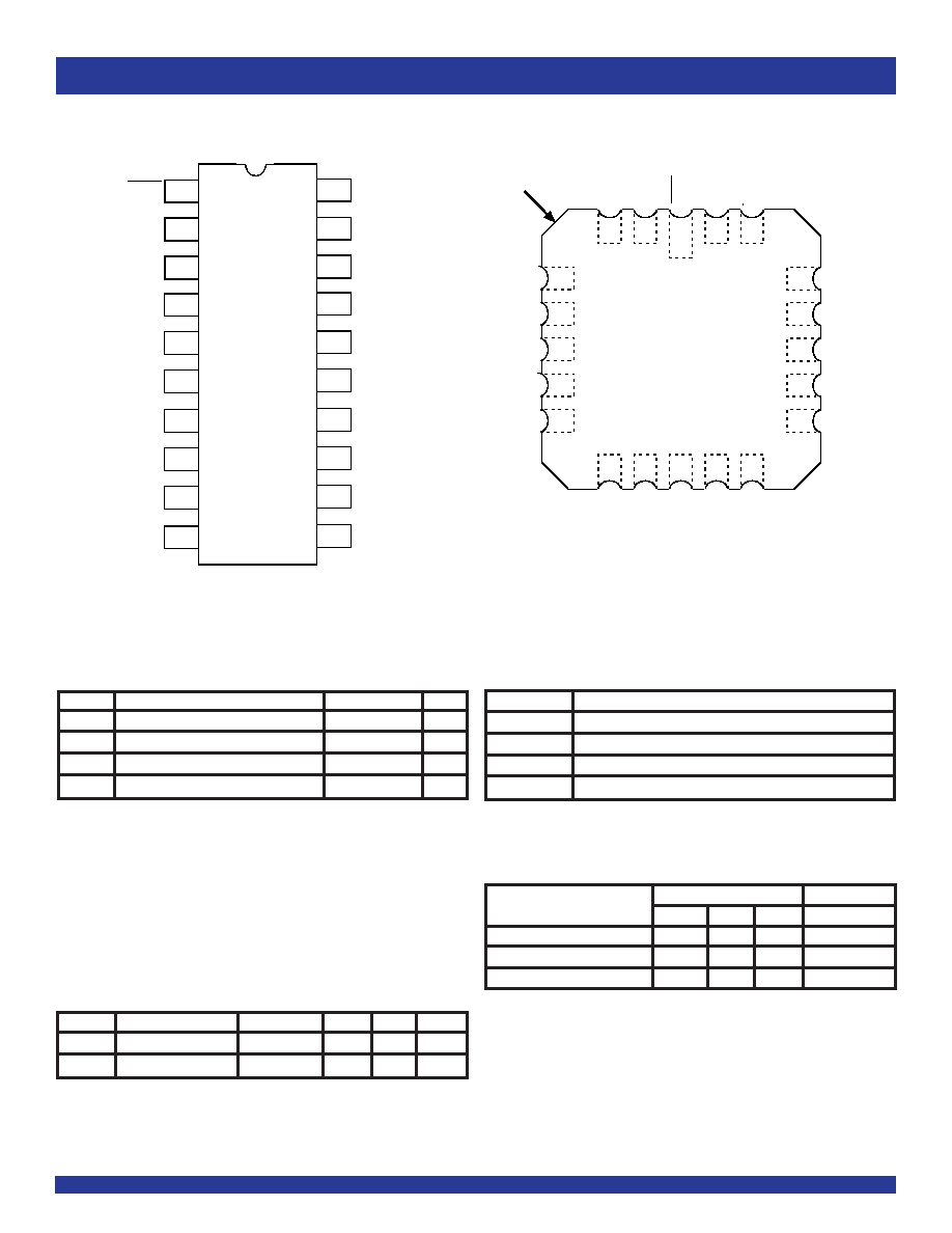
PIN CONFIGURATION
Symbol
Description
Max
Unit
VTERM(2)
Terminal Voltage with Respect to GND
–0.5 to +7
V
VTERM(3)
Terminal Voltage with Respect to GND
–0.5 to VCC+0.5
V
TSTG
Storage Temperature
–65 to +150
° C
IOUT
DC Output Current
–60 to +120
mA
ABSOLUTE MAXIMUM RATINGS(1)
NOTES:
1. Stresses greater than those listed under ABSOLUTE MAXIMUM RATINGS may cause
permanent damage to the device. This is a stress rating only and functional operation
of the device at these or any other conditions above those indicated in the operational
sections of this specification is not implied. Exposure to absolute maximum rating
conditions for extended periods may affect reliability. No terminal voltage may exceed
Vcc by +0.5V unless otherwise noted.
2. Inputs and Vcc terminals only.
3. Output and I/O terminals only.
Pin Names
Description
Dx
Data Inputs
MR
Master Reset (Active LOW)
C P
Clock Pulse Input (Active Rising Edge)
O x
Data Outputs
PIN DESCRIPTION
Symbol
Parameter
(1)
Conditions
Typ.
Max.
Unit
CIN
Input Capacitance
VIN = 0V
6
10
pF
COUT
Output Capacitance
VOUT = 0V
8
12
pF
CAPACITANCE (TA = +25°C, F = 1.0MHz)
NOTE:
1. This parameter is measured at characterization but not tested.
LCC
TOP VIEW
CERDIP/ SOIC/ SSOP/ QSOP
TOP VIEW
FUNCTION TABLE(1)
Inputs
Outputs
Operating Mode
MR
CP
Dx
Ox
Reset (Clear)
L
X
L
Load "1"
L
↑
hH
Load "0"
H
↑
lL
2
3
1
16
15
14
11
19
18
20
17
13
12
5
6
7
4
8
9
10
D1
O0
D0
VCC
O1
D3
O2
D2
O3
GND
O7
O6
D7
D6
O5
O4
D5
D4
CP
MR
1
2
3
4
5
7
9
6
8
10
11
12
13
14
15
16
17
18
19
20
O6
D7
D6
O5
D5
D
0
O
0
O
3
G
N
D
C
P
O
4
D
4
M
R
V
C
O
7
INDEX
D1
O1
D3
O2
D2
NOTE:
1. H = HIGH voltage level steady state
h = HIGH voltage level one set-up time prior to the LOW-to-HIGH clock
transition
L = LOW voltage level steady state
I = LOW voltage level one set-up time prior to the LOW-to-HIGH clock
transition
X = Don’t Care
↑ = LOW-to-HIGH Clock Transition
相关PDF资料 |
PDF描述 |
|---|---|
| IDT74FCT2828ATP | FCT SERIES, 10-BIT DRIVER, INVERTED OUTPUT, PDIP24 |
| IDT54FCT2828ATDB | FCT SERIES, 10-BIT DRIVER, INVERTED OUTPUT, CDIP24 |
| IDT54FCT828ATDB | FCT SERIES, 10-BIT DRIVER, INVERTED OUTPUT, CDIP24 |
| IDT54FCT828CTLB | FCT SERIES, 10-BIT DRIVER, INVERTED OUTPUT, CQCC28 |
| IDT74FCT2828BTSO | FCT SERIES, 10-BIT DRIVER, INVERTED OUTPUT, PDSO24 |
相关代理商/技术参数 |
参数描述 |
|---|---|
| IDT74FCT273ATSO | 制造商:Integrated Device Technology Inc 功能描述: |
| IDT74FCT273HTP | 制造商:Rochester Electronics LLC 功能描述:- Bulk |
| IDT74FCT273P | 制造商:Integrated Device Technology Inc 功能描述: |
| IDT74FCT273TP | 制造商:Integrated Device Technology Inc 功能描述: |
| IDT74FCT273TPY | 制造商:Rochester Electronics LLC 功能描述:- Bulk |
发布紧急采购,3分钟左右您将得到回复。