- 您现在的位置:买卖IC网 > PDF目录65589 > IDT74FST163861PF8 (INTEGRATED DEVICE TECHNOLOGY INC) CBT/FST/QS/5C/B SERIES, DUAL 10-BIT DRIVER, TRUE OUTPUT, PDSO48 PDF资料下载
参数资料
| 型号: | IDT74FST163861PF8 |
| 厂商: | INTEGRATED DEVICE TECHNOLOGY INC |
| 元件分类: | 总线收发器 |
| 英文描述: | CBT/FST/QS/5C/B SERIES, DUAL 10-BIT DRIVER, TRUE OUTPUT, PDSO48 |
| 封装: | TVSOP-48 |
| 文件页数: | 4/6页 |
| 文件大小: | 93K |
| 代理商: | IDT74FST163861PF8 |
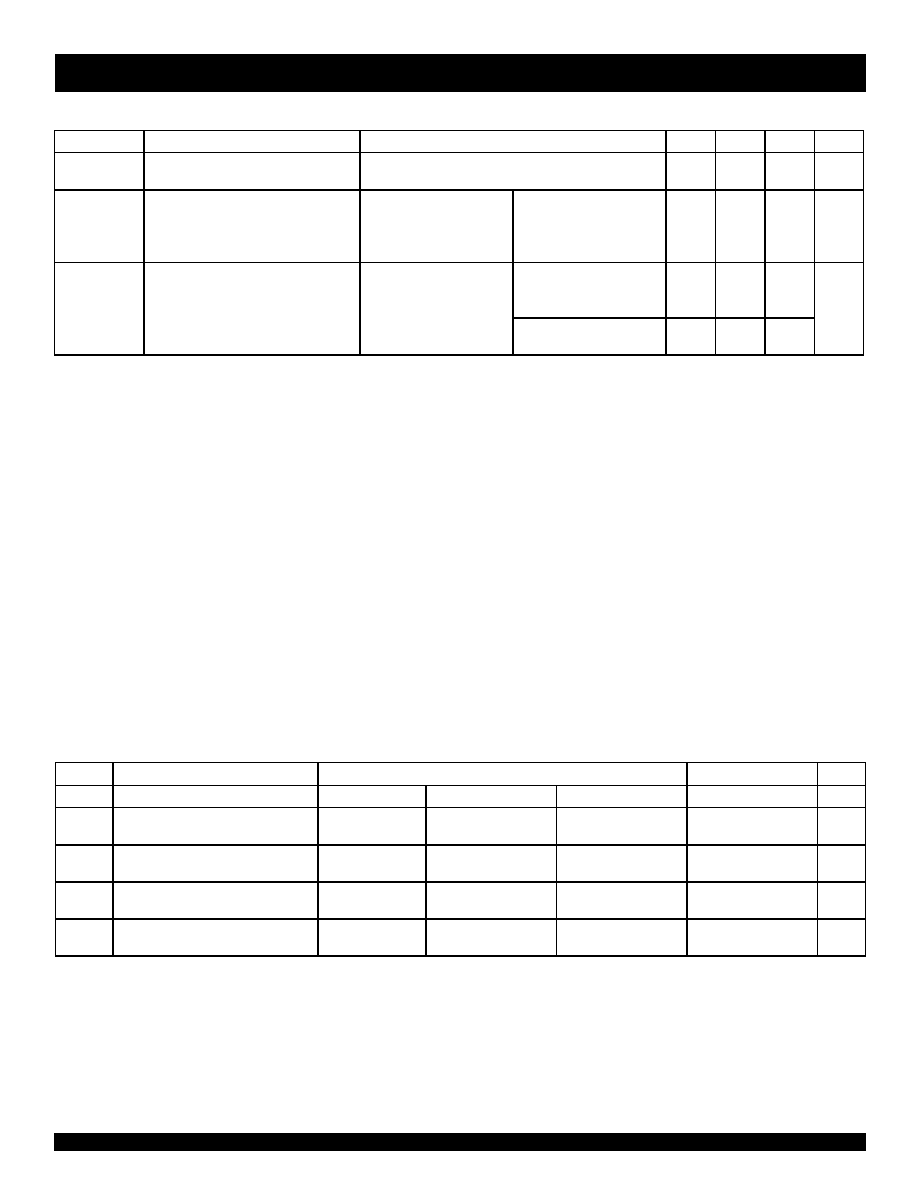
4
INDUSTRIALTEMPERATURERANGE
IDT74FST163861
20-BIT, TWO PORT BUS SWITCH
POWER SUPPLY CHARACTERISTICS
Symbol
Parameter
Test Conditions(1)
Min.
Typ.(2)
Max.
Unit
ICC
Quiescent Power Supply Current
TTL Inputs HIGH
VCC = Max.
VIN = 3.4V(3)
—0.5
1.5
mA
ICCD
Dynamic Power Supply Current(4,5)
VCC = Max.
Outputs Open
VIN = VCC
VIN = GND
—
30
400
A/
MHz/
Enable Pin Toggling
50% Duty Cycle
Enable
IC
Total Power Supply Current(6)
VCC = Max.
Outputs Open
2 Enable Pins Toggling
VIN = VCC
VIN = GND
—0.6
8
mA
fi = 10MHz
50% Duty Cycle
VIN = 3.4
VIN = GND
—0.7
9.5
NOTES:
1. For conditions shown as Max. or Min., use appropriate value specified under Electrical Characteristics for the applicable device type. TA = –40°C to
+85°C
2. Typical values are at VCC = 5.0V, +25°C ambient.
3. Per TTL driven input (VIN = 3.4V). All other inputs at VCC or GND. Switch inputs do not contribute to
ICC.
4. This parameter represents the current required to switch the internal capacitance of the control inputs at the specified frequency.
Switch inputs generate no significant power supply currents as they transition. This parameter is not directly testable, but is derived for use in Total
Power Supply Calculations.
5. CPD = ICCD/VCC
CPD = Power Dissipation Capacitance
6. IC = IQUIESCENT + IINPUTS + IDYNAMIC
IC = ICC +
ICC DHNT + ICCD (fiN)
ICC = Quiescent Current
ICC = Power Supply Current for a TTL High Input (VIN = 3.4V)
DH = Duty Cycle for TTL Inputs High
NT = Number of TTL Inputs at DH
ICCD = Dynamic Current Caused by an Input Transition Pair (HLH or LHL)
fi = Control Input Frequency
N = Number of Control Inputs Toggling at fi
SWITCHING CHARACTERISTICS OVER OPERATING RANGE
Following Conditions Apply Unless Otherwise Specified:
Commercial: TA = -40°C to +85°C, VCC = 5.0V ± 10%
VCC = 5V ± 10%
VCC = 4V
Symbol
Description(1)
Min.
Typ.
Max.
Unit
tPLH
tPHL
Data Propagation Delay
A to B, Y to B(2)
—
0.25
ns
tPZH
tPZL
Switch CONNECT Delay
x
OE to A or B
1.5
—
6.5
7
ns
tPHZ
tPLZ
Switch DISCONNECT Delay
x
OE to A or B
1.5
—
7
ns
|QCI|
Charge Injection During Switch
DISCONNECT, x
OE to A or B(3)
—1.5
—
pC
NOTES:
1. See test circuits and waveforms.
2. The bus switch contributes no Propagation Delay other than the RC Delay of the load interacting with the RC of the switch.
3. |QCI| is the charge injection for a single switch DISCONNECT and applies to either single switches or multiplexers.
|QDCI| is the charge injection for a multiplexer as the multiplexed port switches from one path to another. Charge injection is reduced because the
injection from the DISCONNECT of the first path is compensated by the CONNECT of the second path.
相关PDF资料 |
PDF描述 |
|---|---|
| IDT74FST3125PG8 | CBT/FST/QS/5C/B SERIES, 4-BIT DRIVER, TRUE OUTPUT, PDSO14 |
| IDT74FST32244P | CBT/FST/QS/5C/B SERIES, DUAL 4-BIT DRIVER, TRUE OUTPUT, PDIP20 |
| IDT74FST32244PY | CBT/FST/QS/5C/B SERIES, DUAL 4-BIT DRIVER, TRUE OUTPUT, PDSO20 |
| IDT74FST3244SO | CBT/FST/QS/5C/B SERIES, QUAD 4-BIT DRIVER, TRUE OUTPUT, PDSO20 |
| IDT74FST32XL384PF8 | CBT/FST/QS/5C/B SERIES, DUAL 10-BIT DRIVER, TRUE OUTPUT, PDSO48 |
相关代理商/技术参数 |
参数描述 |
|---|---|
| IDT74FST3125Q | 制造商:Integrated Device Technology Inc 功能描述:BUS Switch, 16 Pin, Plastic, SSOP |
| IDT74FST32383FPG | 制造商:Rochester Electronics LLC 功能描述:- Bulk |
| IDT74FST32384FSO | 制造商:Rochester Electronics LLC 功能描述:- Bulk 制造商:Integrated Device Technology Inc 功能描述: |
| IDT74FST3244FPG | 制造商:Integrated Device Technology Inc 功能描述: |
| IDT74FST3244FSO | 制造商:Rochester Electronics LLC 功能描述:- Bulk |
发布紧急采购,3分钟左右您将得到回复。