- 您现在的位置:买卖IC网 > PDF目录65590 > IDT74FST3125PG8 (INTEGRATED DEVICE TECHNOLOGY INC) CBT/FST/QS/5C/B SERIES, 4-BIT DRIVER, TRUE OUTPUT, PDSO14 PDF资料下载
参数资料
| 型号: | IDT74FST3125PG8 |
| 厂商: | INTEGRATED DEVICE TECHNOLOGY INC |
| 元件分类: | 总线收发器 |
| 英文描述: | CBT/FST/QS/5C/B SERIES, 4-BIT DRIVER, TRUE OUTPUT, PDSO14 |
| 封装: | TSSOP-14 |
| 文件页数: | 3/5页 |
| 文件大小: | 91K |
| 代理商: | IDT74FST3125PG8 |
3
IDT74FST3125
4-BIT BUS SWITCH
COMMERCIALTEMPERATURERANGE
NOTES:
1. For conditions shown as Max. or Min., use appropriate value specified under Electrical Characteristics for the applicable device type.
2. Typical values are at VCC = 5.0V, +25°C ambient.
3. Per TTL driven input (VIN = 3.4V). All other inputs at VCC or GND.
4. This parameter is not directly testable, but is derived for use in Total Power Supply Calculations.
5. IC = IQUIESCENT + IINPUTS + IDYNAMIC
IC = ICC +
ICC DHNT + ICCD (fiN)
ICC = Quiescent Current
ICC = Power Supply Current for a TTL High Input (VIN = 3.4V)
DH = Duty Cycle for TTL Inputs High
NT = Number of TTL Inputs at DH
ICCD = Dynamic Current Caused by an Input Transition Pair (HLH or LHL)
fi = Input Frequency
N = Number of Switches Toggling at fi
All currents are in milliamps and all frequencies are in megahertz.
NOTES:
1. See test circuit and waveforms.
2. Minimum limits guaranteed but not tested.
3. This parameter is guaranteed by design but not tested.
4. The bus switch contributes no propagation delay other than the RC delay of the on resistance of the switch and the load capacitance. The time constant
for the switch alone is of the order of 2.5ns for 50pF load. Since this time is constant and much smaller than the rise/fall times of typical driving signals,
it adds very little propagation delay to the system. Propagation delay on the bus switch when used in a system is determined by the driving circuit on
the driving side of the switch and its interaction with the load on the driven side.
5. Measured at switch turn off, load = 50 pF in parallel with 10M
scope probe, VIN = 0.0 volts.
6. Characterized parameter. Not 100% tested.
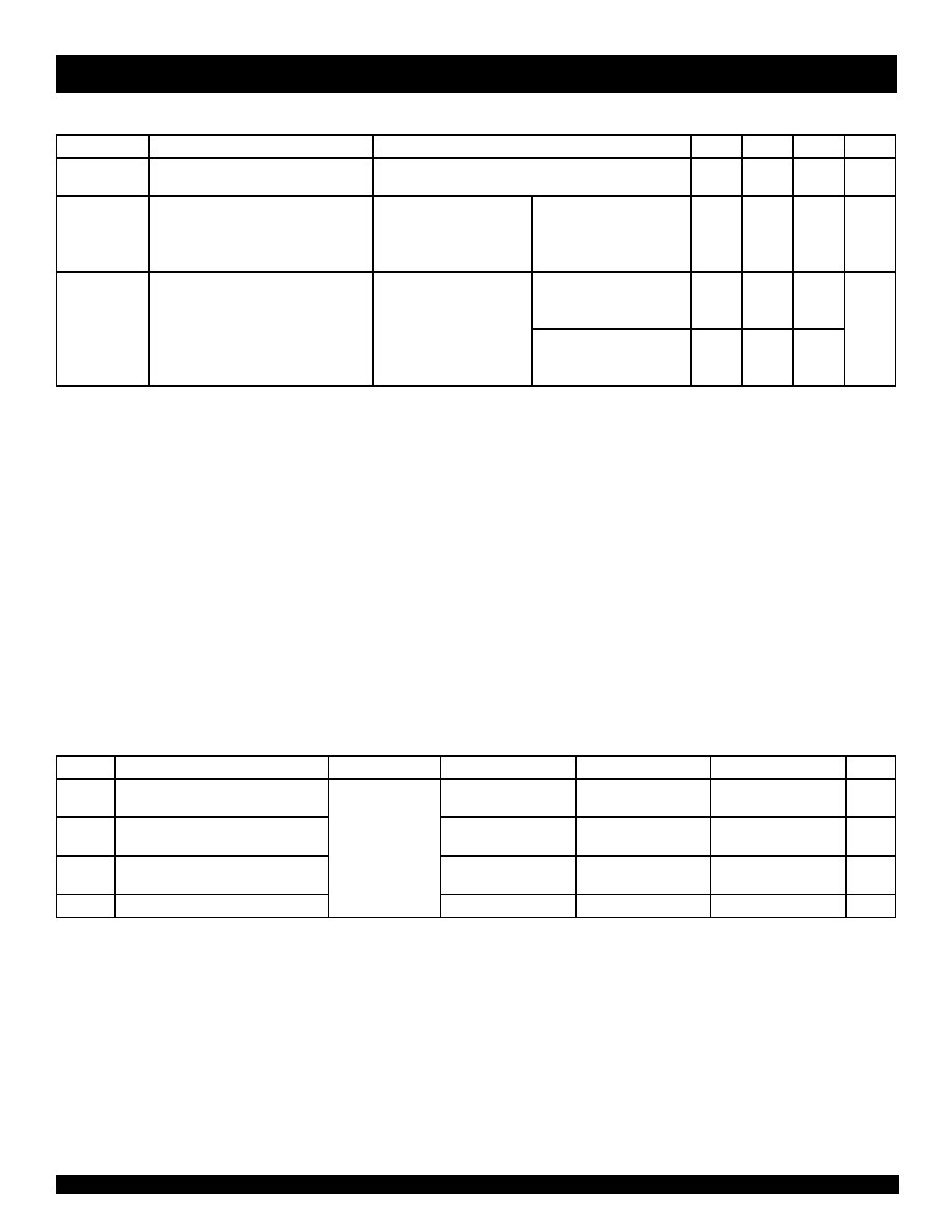
POWER SUPPLY CHARACTERISTICS
Symbol
Parameter
Test Conditions(1)
Min.
Typ.(2)
Max.
Unit
ICC
Quiescent Power Supply Current
TTL Inputs HIGH
VCC = Max.
VIN = 3.4V(3)
—0.5
1.5
mA
ICCD
Dynamic Power Supply Current(4)
VCC = Max.
Outputs Open
VIN = VCC
VIN = GND
—30
40
A/
MHz/
Enable Pin Toggling
50% Duty Cycle
Switch
IC
Total Power Supply Current(5)
VCC = Max.
Outputs Open
Enable Pin Toggling
VIN = VCC
VIN = GND
—1.2
1.6
mA
(4 Switches Toggling)
fi = 10MHz
50% Duty Cycle
VIN = 3.4
VIN = GND
—1.5
2.4
SWITCHING CHARACTERISTICS OVER OPERATING RANGE
Following Conditions Apply Unless Otherwise Specified:
Commercial: TA = -40°C to +85°C, VCC = 5.0V ± 5%
Symbol
Description
Condition(1)
Min.(2)
Typ.
Max.
Unit
tPLH
tPHL
Data Propagation Delay
A to Y, Y to A(3,4)
CL = 50pF
RL = 500
—
0.25
ns
tPZH
tPZL
Switch Turn on Delay
OE to A, Y
1.5
—
6.5
ns
tPHZ
tPLZ
Switch Turn off Delay
OE to A, Y(3)
1.5
—
5.5
ns
|QCI|
Charge Injection(5,6)
—1.5
—
pC
相关PDF资料 |
PDF描述 |
|---|---|
| IDT74FST32244P | CBT/FST/QS/5C/B SERIES, DUAL 4-BIT DRIVER, TRUE OUTPUT, PDIP20 |
| IDT74FST32244PY | CBT/FST/QS/5C/B SERIES, DUAL 4-BIT DRIVER, TRUE OUTPUT, PDSO20 |
| IDT74FST3244SO | CBT/FST/QS/5C/B SERIES, QUAD 4-BIT DRIVER, TRUE OUTPUT, PDSO20 |
| IDT74FST32XL384PF8 | CBT/FST/QS/5C/B SERIES, DUAL 10-BIT DRIVER, TRUE OUTPUT, PDSO48 |
| IDT74FST3390SO8 | CBT/FST/QS/5C/B SERIES, OCTAL MULTIPLEXER, PDSO28 |
相关代理商/技术参数 |
参数描述 |
|---|---|
| IDT74FST3125Q | 制造商:Integrated Device Technology Inc 功能描述:BUS Switch, 16 Pin, Plastic, SSOP |
| IDT74FST32383FPG | 制造商:Rochester Electronics LLC 功能描述:- Bulk |
| IDT74FST32384FSO | 制造商:Rochester Electronics LLC 功能描述:- Bulk 制造商:Integrated Device Technology Inc 功能描述: |
| IDT74FST3244FPG | 制造商:Integrated Device Technology Inc 功能描述: |
| IDT74FST3244FSO | 制造商:Rochester Electronics LLC 功能描述:- Bulk |
发布紧急采购,3分钟左右您将得到回复。