- 您现在的位置:买卖IC网 > PDF目录61088 > IDT74LVC374AP (INTEGRATED DEVICE TECHNOLOGY INC) LVC/LCX/Z SERIES, 8-BIT DRIVER, TRUE OUTPUT, PDSO20 PDF资料下载
参数资料
| 型号: | IDT74LVC374AP |
| 厂商: | INTEGRATED DEVICE TECHNOLOGY INC |
| 元件分类: | 总线收发器 |
| 英文描述: | LVC/LCX/Z SERIES, 8-BIT DRIVER, TRUE OUTPUT, PDSO20 |
| 封装: | TSSOP-20 |
| 文件页数: | 1/6页 |
| 文件大小: | 68K |
| 代理商: | IDT74LVC374AP |
INDUSTRIALTEMPERATURERANGE
IDT74LVC374A
3.3VCMOSOCTALEDGE-TRIGGEREDD-TYPEFLIP-FLOP
1
APRIL 1999
INDUSTRIAL TEMPERATURE RANGE
The IDT logo is a registered trademark of Integrated Device Technology, Inc.
1999 Integrated Device Technology, Inc.
DSC-4618/3
FEATURES:
0.5 MICRON CMOS Technology
ESD > 2000V per MIL-STD-883, Method 3015; > 200V using
machine model (C = 200pF, R = 0)
VCC = 3.3V ± 0.3V, Normal Range
VCC = 2.7V to 3.6V, Extended Range
CMOS power levels (0.4
μμμμμ W typ. static)
Rail-to-rail output swing for increased noise margin
All inputs, outputs, and I/O are 5V tolerant
Supports hot insertion
Available in SOIC, SSOP, QSOP, and TSSOP packages
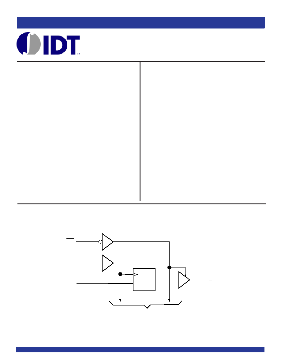
FUNCTIONAL BLOCK DIAGRAM
APPLICATIONS:
5V and 3.3V mixed voltage systems
Data communication and telecommunication systems
DRIVE FEATURES:
High Output Drivers: ±24mA
Reduced system switching noise
IDT74LVC374A
DESCRIPTION:
The LVC374A octal edge triggered D-type flip-flop is built using advanced
dual metal CMOS technology. This device features 3-state outputs designed
specifically for driving highly capacitive or relatively low-impedance loads.
The LVC374A device is particularly suitable for implementing buffer regis-
ters, input-output (I/O) ports, bidirectional bus drivers, and working regis-
ters.
On the positive transition of the clock (CLK) input, the Q outputs are set
to the logic levels set up at the data (D) inputs.
A buffered output-enable (
OE) input can be used to place the eight outputs
in either a normal logic state (high or low logic levels) or a high-impedance
state. In the high-impedance state, the outputs neither load nor drive the bus
lines significantly. The high-impedance state and increased drive provide
the capability to drive bus lines without interface or pullup components.
OE
does not affect internal operations of the latch. Old data can be retained or
new data can be entered while the outputs are in the high-impedance state.
The LVC374A has been designed with a ±24mA output driver. This
driver is capable of driving a moderate to heavy load while maintaining
speed performance.
To ensure the high-impedance state during power up or power down,
OE
should be tied to VCC through a pullup resistor; the minimum value of the
resistor is determined by the current-sinking capability of the driver.
Inputs can be driven from either 3.3V or 5V devices. This feature allows
the use of this device as a translator in a mixed 3.3V/5V system environment.
3.3V CMOS OCTAL
EDGE-TRIGGERED D-TYPE FLIP-
FLOP WITH 3-STATE OUTPUTS
AND 5 VOLT TOLERANT I/O
OE
C1
CLK
1
D
TO SEVEN OTHER CHANNELS
1
11
3
2
1
D
1
Q
相关PDF资料 |
PDF描述 |
|---|---|
| IDT74LVC374APY8 | LVC/LCX/Z SERIES, 8-BIT DRIVER, TRUE OUTPUT, PDSO20 |
| IDT74LVC540AQ | LVC/LCX/Z SERIES, 8-BIT DRIVER, INVERTED OUTPUT, PDSO20 |
| IDT74LVC540AQ8 | LVC/LCX/Z SERIES, 8-BIT DRIVER, INVERTED OUTPUT, PDSO20 |
| IDT74LVC541AQG8 | LVC/LCX/Z SERIES, 8-BIT DRIVER, TRUE OUTPUT, PDSO20 |
| IDT74LVC541AQG | LVC/LCX/Z SERIES, 8-BIT DRIVER, TRUE OUTPUT, PDSO20 |
相关代理商/技术参数 |
参数描述 |
|---|---|
| IDT74LVC374APG | 制造商:MAJOR 功能描述: |
| IDT74LVC4245APGG | 功能描述:IC BUS TRANSCVR 3-ST 8B 24TSSOP RoHS:是 类别:集成电路 (IC) >> 逻辑 - 变换器 系列:74LVC 产品培训模块:Lead (SnPb) Finish for COTS Obsolescence Mitigation Program 标准包装:100 系列:- 逻辑功能:变换器,双向 位数:2 输入类型:CMOS 输出类型:CMOS 数据速率:16Mbps 通道数:2 输出/通道数目:1 差分 - 输入:输出:无/无 传输延迟(最大):15ns 电源电压:1.65 V ~ 5.5 V 工作温度:-40°C ~ 85°C 封装/外壳:10-UFQFN 供应商设备封装:10-UTQFN(1.4x1.8) 包装:管件 |
| IDT74LVC4245APGG8 | 功能描述:IC BUS TRANSCVR 3-ST 8B 24TSSOP RoHS:是 类别:集成电路 (IC) >> 逻辑 - 变换器 系列:74LVC 产品培训模块:Lead (SnPb) Finish for COTS Obsolescence Mitigation Program 标准包装:100 系列:- 逻辑功能:变换器,双向 位数:2 输入类型:CMOS 输出类型:CMOS 数据速率:16Mbps 通道数:2 输出/通道数目:1 差分 - 输入:输出:无/无 传输延迟(最大):15ns 电源电压:1.65 V ~ 5.5 V 工作温度:-40°C ~ 85°C 封装/外壳:10-UFQFN 供应商设备封装:10-UTQFN(1.4x1.8) 包装:管件 |
| IDT74LVC4245APYG | 功能描述:IC BUS TRANSCVR 3-ST 8BIT 24SSOP RoHS:是 类别:集成电路 (IC) >> 逻辑 - 变换器 系列:74LVC 产品培训模块:Lead (SnPb) Finish for COTS Obsolescence Mitigation Program 标准包装:100 系列:- 逻辑功能:变换器,双向 位数:2 输入类型:CMOS 输出类型:CMOS 数据速率:16Mbps 通道数:2 输出/通道数目:1 差分 - 输入:输出:无/无 传输延迟(最大):15ns 电源电压:1.65 V ~ 5.5 V 工作温度:-40°C ~ 85°C 封装/外壳:10-UFQFN 供应商设备封装:10-UTQFN(1.4x1.8) 包装:管件 |
| IDT74LVC4245APYG8 | 功能描述:IC BUS TRANSCVR 3-ST 8BIT 24SSOP RoHS:是 类别:集成电路 (IC) >> 逻辑 - 变换器 系列:74LVC 产品培训模块:Lead (SnPb) Finish for COTS Obsolescence Mitigation Program 标准包装:100 系列:- 逻辑功能:变换器,双向 位数:2 输入类型:CMOS 输出类型:CMOS 数据速率:16Mbps 通道数:2 输出/通道数目:1 差分 - 输入:输出:无/无 传输延迟(最大):15ns 电源电压:1.65 V ~ 5.5 V 工作温度:-40°C ~ 85°C 封装/外壳:10-UFQFN 供应商设备封装:10-UTQFN(1.4x1.8) 包装:管件 |
发布紧急采购,3分钟左右您将得到回复。