- 您现在的位置:买卖IC网 > PDF目录131796 > IDT74LVCH373APG (INTEGRATED DEVICE TECHNOLOGY INC) LVC/LCX/Z SERIES, 8-BIT DRIVER, TRUE OUTPUT, PDSO20 PDF资料下载
参数资料
| 型号: | IDT74LVCH373APG |
| 厂商: | INTEGRATED DEVICE TECHNOLOGY INC |
| 元件分类: | 总线收发器 |
| 英文描述: | LVC/LCX/Z SERIES, 8-BIT DRIVER, TRUE OUTPUT, PDSO20 |
| 封装: | 0.65 MM PITCH, TSSOP-20 |
| 文件页数: | 1/6页 |
| 文件大小: | 63K |
| 代理商: | IDT74LVCH373APG |
1
EXTENDEDCOMMERCIALTEMPERATURERANGE
IDT74LVCH373A
3.3V CMOS OCTAL TRANSPARENT D-TYPE LATCH
OCTOBER 1999
1999
Integrated Device Technology, Inc.
DSC-4630/-
c
IDT74LVCH373A
EXTENDED COMMERCIAL TEMPERATURE RANGE
FEATURES:
– 0.5 MICRON CMOS Technology
– ESD > 2000V per MIL-STD-883, Method 3015;
> 200V using machine model (C = 200pF, R = 0)
– 1.27mm pitch SOIC, 0.65mm pitch SSOP,
0.635mm pitch QSOP, 0.65mm pitch TSSOP packages
– Extended commercial range of – 40°C to +85°C
–VCC = 3.3V ±0.3V, Normal Range
–VCC = 2.3V to 3.6V, Extended Range
– CMOS power levels (0.4W typ. static)
– Rail-to-Rail output swing for increased noise margin
– All inputs, outputs and I/O are 5 Volt tolerant
– Supports hot insertion
3.3V CMOS OCTAL
TRANSPARENT D-TYPE LATCH
WITH 3-STATE OUTPUTS, 5 VOLT
TOLERANT I/O AND BUS-HOLD
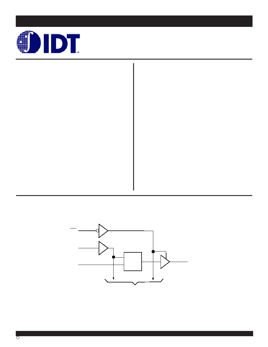
OE
C1
LE
1
D
TO SEVEN OTHER CHANNELS
1
11
3
2
1
D
1
Q
Drive Features for LVCH373A:
– High Output Drivers:
±24mA
– Reduced system switching noise
APPLICATIONS:
5V and 3.3V mixed voltage systems
Data communication and telecommunication systems
NO
T RECOMMENDED
FOR
NEW
DESIGNS
FOR
NEW
DESIGNS
FOR
NEW
DESIGNS
FOR
NEW
DESIGNS
FOR
NEW
DESIGNS
DESCRIPTION:
The LVCH373A octal transparent D-type latch is built using advanced
dual metal CMOS technology. While the latch-enable (LE) input is high, the
Q outputs follow the data (D) inputs. When LE is taken low, the Q outputs
are latched at the logic levels set up at the D inputs.
A buffered output-enable (OE) input can be used to place the eight
outputs in either a normal logic state (high or low logic levels) or a high-
impedance state. In the high-impedance state, the outputs neither load nor
drive the bus lines significantly. OE does not affect the internal operations
of the latches. Old data can be retained or new data can be entered while
the outputs are in the high-impedance state.
The LVCH373A has been designed with a ±24mA output driver. This
driver is capable of driving a moderate to heavy load while maintaining
speed performance.
Inputs can be driven from either 3.3V or 5V devices. This feature allows
the use of this device as a translator in a mixed 3.3V/5V system environ-
ment.
The LVCH373A has “bus-hold” which retains the inputs’ last state
whenever the input goes to a high impedance. This prevents floating inputs
and eliminates the need for pull-up/down resistors.
FUNCTIONAL BLOCK DIAGRAM
相关PDF资料 |
PDF描述 |
|---|---|
| IDTQS33X2253Q18 | HEX MULTIPLEXER, PDSO48 |
| ICS8516FY-01 | LOW SKEW CLOCK DRIVER, 16 TRUE OUTPUT(S), 0 INVERTED OUTPUT(S), PQFP48 |
| ICS8516FY-01T | LOW SKEW CLOCK DRIVER, 16 TRUE OUTPUT(S), 0 INVERTED OUTPUT(S), PQFP48 |
| ICS8516FY-01LF | LOW SKEW CLOCK DRIVER, 16 TRUE OUTPUT(S), 0 INVERTED OUTPUT(S), PQFP48 |
| ICS8516FY-01T | LOW SKEW CLOCK DRIVER, 16 TRUE OUTPUT(S), 0 INVERTED OUTPUT(S), PQFP48 |
相关代理商/技术参数 |
参数描述 |
|---|---|
| IDT74LVCHR162245APA | 制造商:Integrated Device Technology Inc 功能描述: |
| IDT74LVCHR162245APAG | 功能描述:IC BUS TRSCVR 3-ST 16BIT 48TSSOP RoHS:是 类别:集成电路 (IC) >> 逻辑 - 缓冲器,驱动器,接收器,收发器 系列:74LVCHR 标准包装:47 系列:74LVX 逻辑类型:缓冲器/线路驱动器,非反相 元件数:4 每个元件的位元数:1 输出电流高,低:4mA,4mA 电源电压:2 V ~ 3.6 V 工作温度:-40°C ~ 85°C 安装类型:表面贴装 封装/外壳:14-SOIC(0.209",5.30mm 宽) 供应商设备封装:14-SOIC 包装:管件 |
| IDT74LVCHR162245APAG8 | 功能描述:IC BUS TRSCVR 3-ST 16BIT 48TSSOP RoHS:是 类别:集成电路 (IC) >> 逻辑 - 缓冲器,驱动器,接收器,收发器 系列:74LVCHR 产品培训模块:Logic Packages 标准包装:39 系列:74AVCH 逻辑类型:收发器,非反相 元件数:2 每个元件的位元数:8 输出电流高,低:12mA,12mA 电源电压:1.2 V ~ 3.6 V 工作温度:-40°C ~ 85°C 安装类型:表面贴装 封装/外壳:48-TFSOP(0.240",6.10mm 宽) 供应商设备封装:48-TSSOP 包装:管件 产品目录页面:831 (CN2011-ZH PDF) 其它名称:568-2585-574AVCH16245DGG,512935266779512 |
| IDT74LVCHR16646APAG | 功能描述:IC SERIAL RTC LP W/I2C 56-TSSOP RoHS:是 类别:未定义的类别 >> 其它 系列:* 标准包装:1 系列:* 其它名称:MS305720A |
| IDT74LVCHR16646APAG8 | 功能描述:IC SERIAL RTC LP W/I2C 56-TSSOP RoHS:是 类别:未定义的类别 >> 其它 系列:* 标准包装:1 系列:* 其它名称:MS305720A |
发布紧急采购,3分钟左右您将得到回复。