- 您现在的位置:买卖IC网 > PDF目录377488 > IDT82V3010 (Integrated Device Technology, Inc.) T1/E1/OC3 TELECOM CLOCK GENERATOR WITH DUAL REFERENCE INPUTS PDF资料下载
参数资料
| 型号: | IDT82V3010 |
| 厂商: | Integrated Device Technology, Inc. |
| 英文描述: | T1/E1/OC3 TELECOM CLOCK GENERATOR WITH DUAL REFERENCE INPUTS |
| 中文描述: | T1/E1/OC3电信时钟发生器,双基准输入 |
| 文件页数: | 10/31页 |
| 文件大小: | 355K |
| 代理商: | IDT82V3010 |
第1页第2页第3页第4页第5页第6页第7页第8页第9页当前第10页第11页第12页第13页第14页第15页第16页第17页第18页第19页第20页第21页第22页第23页第24页第25页第26页第27页第28页第29页第30页第31页
IDT82V3010
T1/E1/OC3 Telecom Clock Generator with Dual Reference Inputs
Functional Description
10
June 19, 2006
The mode changes between Normal (S1) and Auto-Holdover (S2)
are triggered by the Invalid Input Reference Detection Circuit and are
irrelative to the logic levels on the MODE_sel0 and MODE_sel1 pins. At
the stage of S1, if the input reference is invalid (out of the capture
range), the operating mode will be changed to Auto-Holdover (S2)
automatically. At the stage of S2, if no IN_sel transient occurs and the
input reference becomes valid, the operating mode will be changed back
to Normal (S1) automatically. If an IN_sel transient is detected at the
stage of S2, the operating mode will be changed to Short Time Holdover
(S4) with the TIE Control Block automatically disabled. Refer to
“2.5
Invalid Input Signal Detection”
for more information.
The mode changes between Normal (S1) and Short Time Holdover
(S4) are triggered by the IN_sel transient. At the stage of S1, if a voltage
transient occurs on the IN_sel pin, the operating mode will be changed
to Short Time Holdover (S4) automatically. At the stage of S4, if no
voltage transient occurs on the IN_sel pin, the operating mode will be
changed back to S1 automatically. See
“2.3 Reference Input Switch”
for
details.
When the operating mode is changed from one to another, the TIE
control block is automatically disabled as shown in
Figure - 3
, except the
changes from Short Time Holdover (S4), Holdover (S3) or Auto-
Holdover (S2) to Normal (S1). In the case of changing from S4, S3 or S2
to S1, the TIE control block is enabled or disabled by the TIE_en pin.
2.1.1
NORMAL MODE
The Normal mode is typically used when a slave clock source
synchronized to the network is required.
I
n this mode, the IDT82V3010 provides timing (C1.5o,
C3o
, C2o,
C4o
, C8o,
C16o
, C19o,
C32o
) and synchronization (
F0o
, F8o,
F16o
,
F19o,
F32o
, TSP, RSP) signals. All these signals are synchronous to
one of the two input references. The nominal frequency of the input
reference can be 8 kHz, 1.544 MHz, 2.048 MHz or 19.44 MHz.
After reset, the IDT82V3010 will take 30 seconds at most to make
the output signals synchronous (phase locked) to the input reference.
Whenever the IDT82V3010 works in the Normal mode, the NORMAL
pin will be set to logic high.
2.1.2
FAST LOCK MODE
The Fast Lock mode is a submode of the Normal mode. It allows the
DPLL to lock to a reference more quickly than the Normal mode allows.
Typically, the locking time in the Fast Lock mode is less than 500 ms.
When the FLOCK pin is set to high, the Fast Lock mode will be
enabled.
2.1.3
HOLDOVER MODE
The Holdover mode is typically used for short duration (e.g., 2
seconds) while network synchronization is temporarily disrupted.
In the Holdover mode, the IDT82V3010 provides timing and
synchronization signals that are not locked to an external reference
signal, but are based on storage techniques. In the Normal mode, when
the output frequency is locked to the input reference signal, a numerical
value corresponding to the output frequency is stored alternately in two
memory locations every 30 ms. When the device is changed to the
Holdover mode, the stored value from between 30 ms and 60 ms is used
to set the output frequency of the device.
Whenever the IDT82V3010 works in the Holdover mode, the
HOLDOVER pin will be set to logic high.
2.1.4
FREERUN MODE
The Freerun mode is typically used when a master clock source is
required, or used when a system is just powered up and the network
synchronization has not been achieved.
In this mode, the IDT82V3010 provides timing and synchronization
signals which are based on the master clock frequency (OSCi) only, and
are not synchronized to the input reference signal.
The accuracy of the output clock is equal to the accuracy of the
master clock (OSCi). So if a ±32 ppm output clock is required, the
master clock must also be ±32 ppm. Refer to
“2.8 OSC”
for more
information.
Whenever the IDT82V3010 works in the Freerun mode, the
FREERUN pin will be set to logic high.
2.2
FREQUENCY SELECT CIRCUIT
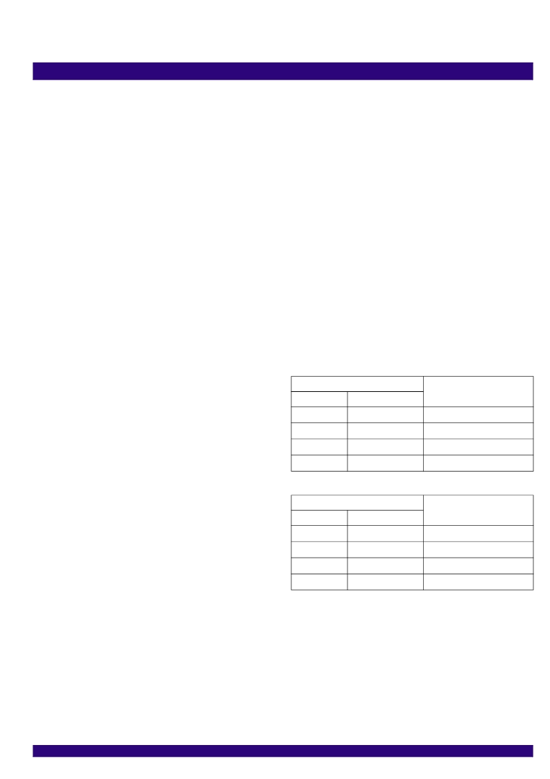
The input reference can be 8 kHz, 1.544 MHz, 2.048 MHz or 19.44
MHz. The F0_sel1 and F0_sel0 pins select one of the four frequencies
for the reference input 0 (Fref0). The F1_sel1 and F1_sel0 pins select
one of the four frequencies for the reference input 1 (Fref1). See
Table -
2
and
Table - 3
for details.
The reference inputs Fref0 and Fref1 may have different frequencies
applied to them. Every time the frequency is changed, the device must
be reset to make the change effective.
2.3
REFERENCE INPUT SWITCH
The IDT82V3010 accepts two simultaneous reference signals Fref0
and Fref1, and operates on the falling edge (8 kHZ, 1.544 MHz and
2.048 MHz) or rising edge (19.44 MHz). One of the two reference
signals will be input to the device, as determined by the IN_sel pin. See
Table - 4
. The selected reference signal is sent to the TIE control block,
Table - 2 Fref0 Frequency Selection
Frequency Selection Pins
Fref0 Input Frequency
F0_sel1
F0_sel0
0
0
19.44 MHz
0
1
8 kHz
1
0
1.544 MHz
1
1
2.048 MHz
Table - 3 Fref1 Frequency Selection
Frequency Selection Pins
Fref1 Input Frequency
F1_sel1
F1_sel0
0
0
19.44 MHz
0
1
8 kHz
1
0
1.544 MHz
1
1
2.048 MHz
相关PDF资料 |
PDF描述 |
|---|---|
| IDT82V3010PV | T1/E1/OC3 TELECOM CLOCK GENERATOR WITH DUAL REFERENCE INPUTS |
| IDT82V3010PVG | T1/E1/OC3 TELECOM CLOCK GENERATOR WITH DUAL REFERENCE INPUTS |
| IDT82V3255 | WAN PLL |
| IDT82V3255DK | WAN PLL |
| IDT82V3255DKG | WAN PLL |
相关代理商/技术参数 |
参数描述 |
|---|---|
| IDT82V3010PV | 制造商:IDT 制造商全称:Integrated Device Technology 功能描述:T1/E1/OC3 TELECOM CLOCK GENERATOR WITH DUAL REFERENCE INPUTS |
| IDT82V3010PVG | 功能描述:IC PLL WAN 51/E1/OC3 DUAL 56SSOP RoHS:是 类别:集成电路 (IC) >> 时钟/计时 - 专用 系列:- 标准包装:1,500 系列:- 类型:时钟缓冲器/驱动器 PLL:是 主要目的:- 输入:- 输出:- 电路数:- 比率 - 输入:输出:- 差分 - 输入:输出:- 频率 - 最大:- 电源电压:3.3V 工作温度:0°C ~ 70°C 安装类型:表面贴装 封装/外壳:28-SSOP(0.209",5.30mm 宽) 供应商设备封装:28-SSOP 包装:带卷 (TR) 其它名称:93786AFT |
| IDT82V3010PVG8 | 功能描述:IC PLL WAN 51/E1/OC3 DUAL 56SSOP RoHS:是 类别:集成电路 (IC) >> 时钟/计时 - 专用 系列:- 标准包装:1,500 系列:- 类型:时钟缓冲器/驱动器 PLL:是 主要目的:- 输入:- 输出:- 电路数:- 比率 - 输入:输出:- 差分 - 输入:输出:- 频率 - 最大:- 电源电压:3.3V 工作温度:0°C ~ 70°C 安装类型:表面贴装 封装/外壳:28-SSOP(0.209",5.30mm 宽) 供应商设备封装:28-SSOP 包装:带卷 (TR) 其它名称:93786AFT |
| IDT82V3011 | 制造商:IDT 制造商全称:Integrated Device Technology 功能描述:T1/E1/OC3 WAN PLL WITH SINGLE REFERENCE INPUT |
| IDT82V3011PV | 制造商:INT_DEV_TECH 功能描述: |
发布紧急采购,3分钟左右您将得到回复。