- 您现在的位置:买卖IC网 > PDF目录9070 > IDTCSP2510DPGG8 (IDT, Integrated Device Technology Inc)IC CLK DVR PLL ZDB 1:10 24TSSOP PDF资料下载
参数资料
| 型号: | IDTCSP2510DPGG8 |
| 厂商: | IDT, Integrated Device Technology Inc |
| 文件页数: | 1/9页 |
| 文件大小: | 0K |
| 描述: | IC CLK DVR PLL ZDB 1:10 24TSSOP |
| 标准包装: | 3,000 |
| 类型: | 驱动器,PLL,零延迟缓冲器 |
| PLL: | 带旁路 |
| 输入: | 时钟 |
| 输出: | 时钟 |
| 电路数: | 1 |
| 比率 - 输入:输出: | 1:10 |
| 差分 - 输入:输出: | 无/无 |
| 频率 - 最大: | 175MHz |
| 除法器/乘法器: | 无/无 |
| 电源电压: | 3 V ~ 3.6 V |
| 工作温度: | 0°C ~ 85°C |
| 安装类型: | 表面贴装 |
| 封装/外壳: | 24-TSSOP(0.173",4.40mm 宽) |
| 供应商设备封装: | 24-TSSOP |
| 包装: | 带卷 (TR) |
| 其它名称: | CSP2510DPGG8 |
1
0
°CTO85°CTEMPERATURERANGE
IDTCSP2510D
3.3V PHASE-LOCK LOOP CLOCK DRIVER
OCTOBER 2001
2001 Integrated Device Technology, Inc.
DSC-5874/3
c
IDTCSP2510D
0C TO 85C TEMPERATURE RANGE
3.3V PHASE-LOCK LOOP
CLOCK DRIVER
ZERO DELAY BUFFER
DESCRIPTION:
The CSP2510D is a high performance, low-skew, low-jitter, phase-lock
loop (PLL) clock driver. It uses a PLL to precisely align, in both frequency
and phase, the feedback (FBOUT) output to the clock (CLK) input signal.
It is specifically designed for use with synchronous DRAMs. The CSP2510D
operates at 3.3V.
One bank of ten outputs provide low-skew, low-jitter copies of CLK.
Output signal duty cycles are adjusted to 50 percent, independent of the duty
cycle at CLK. The outputs can be enabled or disabled via the control G input.
When the G input is high, the outputs switch in phase and frequency with
CLK; when the G input is low, the outputs are disabled to the logic-low state.
Unlike many products containing PLLs, the CSP2510D does not require
external RC networks. The loop filter for the PLL is included on-chip,
minimizing component count, board space, and cost.
Because it is based on PLL circuitry, the CSP2510D requires a
stabilization time to achieve phase lock of the feedback signal to the
reference signal. This stabilization time is required, following power up and
application of a fixed-frequency, fixed-phase signal at CLK, as well as
following any changes to the PLL reference or feedback signals. The PLL
can be bypassed for the test purposes by strapping AVDD to ground.
The CSP2510D is specified for operation from 0°C to +85°C. This device
is also available (on special order) in Industrial temperature range (-40°C
to +85°C). See ordering information for details.
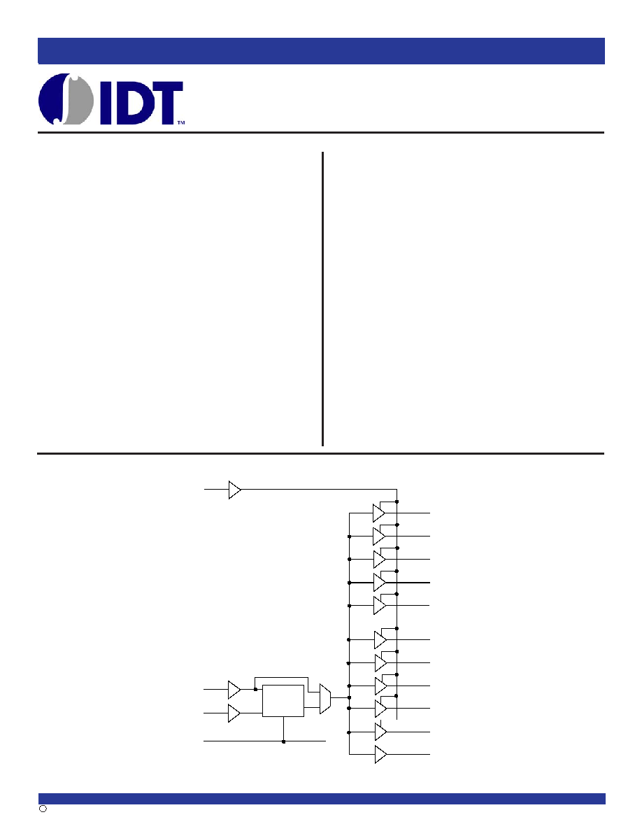
21
Y9
PLL
3
5
8
9
4
Y0
Y1
Y2
Y3
Y4
15
17
20
16
Y5
Y6
Y7
Y8
24
13
23
AVDD
FBIN
CLK
G
11
12
FBOUT
FUNCTIONAL BLOCK DIAGRAM
The IDT logo is a registered trademark of Integrated Device Technology, Inc.
FEATURES:
Phase-Lock Loop Clock Distribution for Synchronous DRAM
Applications
Distributes one clock input to one bank of ten outputs
Output enable bank control
External feedback (FBIN) pin is used to synchronize the
outputs to the clock input signal
No external RC network required for PLL loop stability
Operates at 3.3V VDD
tpd Phase Error at 166MHz: < ±150ps
Jitter (peak-to-peak) at 166MHz: < ±75ps @ 166MHz
Spread Spectrum Compatible
Operating frequency 50MHz to 175MHz
Available in 24-Pin TSSOP package
APPLICATIONS:
SDRAM Modules
PC Motherboards
Workstations
相关PDF资料 |
PDF描述 |
|---|---|
| X9260US24Z-2.7 | IC XDCP DUAL 256TAP 50K 24-SOIC |
| 74AC139SJX | DECODER/DEMUX 1-OF-4 16SOP |
| IDTCSP2510DPG8 | IC CLK DVR PLL ZDB 1:10 24TSSOP |
| X9261TS24Z-2.7 | IC XDCP DUAL 256TAP 100K 24-SOIC |
| ICS501GILFT | IC PLL CLK MULTIPLIER 8-MSOP |
相关代理商/技术参数 |
参数描述 |
|---|---|
| IDTCSP2510DPGGI | 功能描述:IC CLK DVR PLL ZDB 1:10 24TSSOP RoHS:是 类别:集成电路 (IC) >> 时钟/计时 - 时钟发生器,PLL,频率合成器 系列:- 标准包装:1,000 系列:- 类型:时钟/频率合成器,扇出分配 PLL:- 输入:- 输出:- 电路数:- 比率 - 输入:输出:- 差分 - 输入:输出:- 频率 - 最大:- 除法器/乘法器:- 电源电压:- 工作温度:- 安装类型:表面贴装 封装/外壳:56-VFQFN 裸露焊盘 供应商设备封装:56-VFQFP-EP(8x8) 包装:带卷 (TR) 其它名称:844S012AKI-01LFT |
| IDTCSP2510DPGGI8 | 功能描述:IC CLK DVR PLL ZDB 1:10 24TSSOP RoHS:是 类别:集成电路 (IC) >> 时钟/计时 - 时钟发生器,PLL,频率合成器 系列:- 标准包装:1,000 系列:- 类型:时钟/频率合成器,扇出分配 PLL:- 输入:- 输出:- 电路数:- 比率 - 输入:输出:- 差分 - 输入:输出:- 频率 - 最大:- 除法器/乘法器:- 电源电压:- 工作温度:- 安装类型:表面贴装 封装/外壳:56-VFQFN 裸露焊盘 供应商设备封装:56-VFQFP-EP(8x8) 包装:带卷 (TR) 其它名称:844S012AKI-01LFT |
| IDTCSP2510DPGI | 功能描述:IC CLK DVR PLL ZDB 1:10 24TSSOP RoHS:否 类别:集成电路 (IC) >> 时钟/计时 - 时钟发生器,PLL,频率合成器 系列:- 标准包装:1,000 系列:- 类型:时钟/频率合成器,扇出分配 PLL:- 输入:- 输出:- 电路数:- 比率 - 输入:输出:- 差分 - 输入:输出:- 频率 - 最大:- 除法器/乘法器:- 电源电压:- 工作温度:- 安装类型:表面贴装 封装/外壳:56-VFQFN 裸露焊盘 供应商设备封装:56-VFQFP-EP(8x8) 包装:带卷 (TR) 其它名称:844S012AKI-01LFT |
| IDTCSP2510DPGI8 | 功能描述:IC CLK DVR PLL ZDB 1:10 24TSSOP RoHS:否 类别:集成电路 (IC) >> 时钟/计时 - 时钟发生器,PLL,频率合成器 系列:- 标准包装:2,000 系列:- 类型:PLL 时钟发生器 PLL:带旁路 输入:LVCMOS,LVPECL 输出:LVCMOS 电路数:1 比率 - 输入:输出:2:11 差分 - 输入:输出:是/无 频率 - 最大:240MHz 除法器/乘法器:是/无 电源电压:3.135 V ~ 3.465 V 工作温度:0°C ~ 70°C 安装类型:表面贴装 封装/外壳:32-LQFP 供应商设备封装:32-TQFP(7x7) 包装:带卷 (TR) |
| IDTCSP5940Q | 制造商:未知厂家 制造商全称:未知厂家 功能描述:Ten Distributed-Output Clock Driver |
发布紧急采购,3分钟左右您将得到回复。