- 您现在的位置:买卖IC网 > PDF目录377488 > IDTCSPU877ANL (INTEGRATED DEVICE TECHNOLOGY INC) 1.8V PHASE LOCKED LOOP DIFFERENTIAL 1:10 SDRAM CLOCK DRIVER PDF资料下载
参数资料
| 型号: | IDTCSPU877ANL |
| 厂商: | INTEGRATED DEVICE TECHNOLOGY INC |
| 元件分类: | 时钟及定时 |
| 英文描述: | 1.8V PHASE LOCKED LOOP DIFFERENTIAL 1:10 SDRAM CLOCK DRIVER |
| 中文描述: | 877 SERIES, PLL BASED CLOCK DRIVER, 10 TRUE OUTPUT(S), 0 INVERTED OUTPUT(S), PQCC40 |
| 封装: | PLASTIC, MLF-40 |
| 文件页数: | 6/13页 |
| 文件大小: | 139K |
| 代理商: | IDTCSPU877ANL |
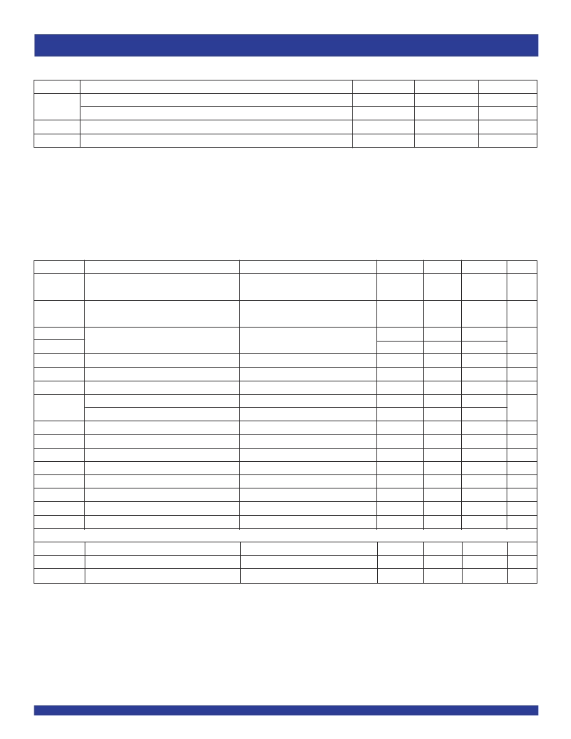
6
COMMERCIAL TEMPERATURE RANGE
IDTCSPU877A
1.8V PLL DIFFERENTIAL 1:10 SDRAM CLOCK DRIVER
TIMING REQUIREMENTS
Symbol
Parameter
f
CLK
Operating Clock Frequency
(1,2)
Application Clock Frequency
(1,3)
t
DC
Input Clock Duty Cycle
t
L
Stabilization Time
(4)
Mn.
125
160
40
Max.
270
270
60
15
Unit
MHz
MHz
%
μ
s
NOTES:
1.
2.
3.
4.
The PLL will track a spread spectrumclock input.
Operating clock frequency is the range over which the PLL will lock, but may not meet all timng specifications. To be used only for low speed systemdebug.
Application clock frequency is the range over which timng specifications apply.
Stabilization time is the time required for the integrated PLL circuit to obtain phase lock of its feedback signal to its reference signal after power up. During normal operation, the
stabilization time is also the time required for the PLL circuit to obtain phase lock of its feedback signal to its reference signal when CLK and
CLK
go to a logic LOW state, enters
the power-down mode, and later return to active operation. CLK and
CLK
may be left floating after they have been driven LOW for one complete clock cycle.
AC ELECTRICAL CHARACTERISTICS
(1)
Symbol
Description
t
PLH(2)
LOW to HIGH Level Propagation Delay Time
Test Conditions
A
VDD
= GND, OE = H, OS = L,
CLK to any output
A
VDD
= GND, OE = H, OS = L,
CLK to any output
166/200/266MHz
Min.
Typ.
(2)
TBD
Max.
Unit
ns
t
PHL(2)
HIGH to LOW Level Propagation Delay Time
TBD
ns
t
JIT(CC+)
t
JIT(CC-)
t
JIT(PER)(3)
t
JIT(HPER)(3)
t
SLR(O)(1,4)
t
SLR(I)(1,4)
Jitter (cycle-to-cycle)
0
0
40
-40
40
60
3
4
50
50
40
8
8
ps
Jitter (period)
Half-Period Jitter
Output Clock Slew Rate (single-ended)
Output Enable (OE)
Input Clock Slew Rate
Static Phase Offset
Dynamc Phase Offset
Output Skew
Output Enable to any Y or
Y
Output Disable to any Y or
Y
AC Differential Output Crosspoint Voltage
AC Differential Input Voltage
AC Differential Input Crosspoint Voltage
The PLL on the CSPU877A will meet all the above test parameters while supporting SSC synthesizers with the following parameters:
SSC
Modulation Frequency
SSC
Clock Input Frequency Deviation
f
3dB
PLL Loop Bandwidth
166/200/266MHz
166/200/266MHz
166/200/266MHz (20% to 80%)
-40
-60
1.5
0.5
1
-50
-50
ps
ps
V/ns
V/ns
2.5
2.5
t
(
)(5)
t
(
)DYN
t
SK(O)
t
EN
t
DIS
V
OX(6)
V
ID(AC)
V
IX
166/200/266MHz
166/200/266MHz
ps
ps
ps
ns
ns
V
V
V
Differential outputs termnated with 120
(V
DDQ
/2) -0.1
0.6
(V
DDQ
/2) -0.15
(V
DDQ
/2) +0.1
V
DDQ
+0.4
(V
DDQ
/2) +0.15
30
0
2
33
-0.5
KHz
%
MHz
NOTES:
1. There are two different termnations that are used with the above AC tests. The output load shown in figure 1 is used to measure the input and output differential pair cross-voltage
only. The output load shown in figure 2 is used to measure all other tests, including input and output slew rates. For consistency, use 50
equal length cables with SMA connectors
on the test board.
2. Refers to transition of non-inverting output.
3. Period jitter and half-period jitter specifications are seperate specifications that must be met independently of each other.
4. To elimnate the impact of input slew rates on static phase offset, the input slew rates of reference clock input (CLK,
CLK
) and feedback clock input (FBIN,
FBIN
) are recommended
to be nearly equal. The 2.5V/ns slew rates are shown as a recommended target. Compliance with these nomnal values is not mandatory if it can be adequately demonstrated
that alternative characteristics meet the requirements of the registered DDR2 DIMMapplication.
5. Static phase offset does not include jitter.
6. V
OX
is specified at the DDR DRAMclock input or test load.
相关PDF资料 |
PDF描述 |
|---|---|
| IDTCSPU877ANLG | 1.8V PHASE LOCKED LOOP DIFFERENTIAL 1:10 SDRAM CLOCK DRIVER |
| IDTCSPU877A | 1.8V PHASE LOCKED LOOP DIFFERENTIAL 1:10 SDRAM CLOCK DRIVER |
| IDTCSPU877ABV | 1.8V PHASE LOCKED LOOP DIFFERENTIAL 1:10 SDRAM CLOCK DRIVER |
| IDTCSPU877D | 1.8V PHASE LOCKED LOOP DIFFERENTIAL 1:10 SDRAM CLOCK DRIVER |
| IDTCSPU877DBV | 1.8V PHASE LOCKED LOOP DIFFERENTIAL 1:10 SDRAM CLOCK DRIVER |
相关代理商/技术参数 |
参数描述 |
|---|---|
| IDTCSPU877ANLG | 功能描述:IC PLL CLK DVR SDRAM 40-VFQFPN RoHS:是 类别:集成电路 (IC) >> 时钟/计时 - 专用 系列:- 标准包装:28 系列:- 类型:时钟/频率发生器 PLL:是 主要目的:Intel CPU 服务器 输入:时钟 输出:LVCMOS 电路数:1 比率 - 输入:输出:3:22 差分 - 输入:输出:无/是 频率 - 最大:400MHz 电源电压:3.135 V ~ 3.465 V 工作温度:0°C ~ 85°C 安装类型:表面贴装 封装/外壳:64-TFSOP (0.240",6.10mm 宽) 供应商设备封装:64-TSSOP 包装:管件 |
| IDTCSPU877ANLG8 | 功能描述:IC PLL CLK DVR SDRAM 40-VFQFPN RoHS:是 类别:集成电路 (IC) >> 时钟/计时 - 专用 系列:- 标准包装:28 系列:- 类型:时钟/频率发生器 PLL:是 主要目的:Intel CPU 服务器 输入:时钟 输出:LVCMOS 电路数:1 比率 - 输入:输出:3:22 差分 - 输入:输出:无/是 频率 - 最大:400MHz 电源电压:3.135 V ~ 3.465 V 工作温度:0°C ~ 85°C 安装类型:表面贴装 封装/外壳:64-TFSOP (0.240",6.10mm 宽) 供应商设备封装:64-TSSOP 包装:管件 |
| IDTCSPU877BVG | 功能描述:IC PLL CLK DVR SDRAM 56-CABGA RoHS:是 类别:集成电路 (IC) >> 时钟/计时 - 专用 系列:- 标准包装:28 系列:- 类型:时钟/频率发生器 PLL:是 主要目的:Intel CPU 服务器 输入:时钟 输出:LVCMOS 电路数:1 比率 - 输入:输出:3:22 差分 - 输入:输出:无/是 频率 - 最大:400MHz 电源电压:3.135 V ~ 3.465 V 工作温度:0°C ~ 85°C 安装类型:表面贴装 封装/外壳:64-TFSOP (0.240",6.10mm 宽) 供应商设备封装:64-TSSOP 包装:管件 |
| IDTCSPU877BVG8 | 功能描述:IC PLL CLK DVR SDRAM 56-CABGA RoHS:是 类别:集成电路 (IC) >> 时钟/计时 - 专用 系列:- 标准包装:28 系列:- 类型:时钟/频率发生器 PLL:是 主要目的:Intel CPU 服务器 输入:时钟 输出:LVCMOS 电路数:1 比率 - 输入:输出:3:22 差分 - 输入:输出:无/是 频率 - 最大:400MHz 电源电压:3.135 V ~ 3.465 V 工作温度:0°C ~ 85°C 安装类型:表面贴装 封装/外壳:64-TFSOP (0.240",6.10mm 宽) 供应商设备封装:64-TSSOP 包装:管件 |
| IDTCSPU877D | 制造商:IDT 制造商全称:Integrated Device Technology 功能描述:1.8V PHASE LOCKED LOOP DIFFERENTIAL 1:10 SDRAM CLOCK DRIVER |
发布紧急采购,3分钟左右您将得到回复。