- 您现在的位置:买卖IC网 > PDF目录67123 > IDTQS74FCT2573ATSO (INTEGRATED DEVICE TECHNOLOGY INC) FCT SERIES, 8-BIT DRIVER, TRUE OUTPUT, PDSO20 PDF资料下载
参数资料
| 型号: | IDTQS74FCT2573ATSO |
| 厂商: | INTEGRATED DEVICE TECHNOLOGY INC |
| 元件分类: | 总线收发器 |
| 英文描述: | FCT SERIES, 8-BIT DRIVER, TRUE OUTPUT, PDSO20 |
| 封装: | SOIC-20 |
| 文件页数: | 3/6页 |
| 文件大小: | 54K |
| 代理商: | IDTQS74FCT2573ATSO |
3
IDTQS74FCT2573T/AT
HIGH-SPEEDCMOSBUSINTERFACE8-BITLATCH
INDUSTRIALTEMPERATURERANGE
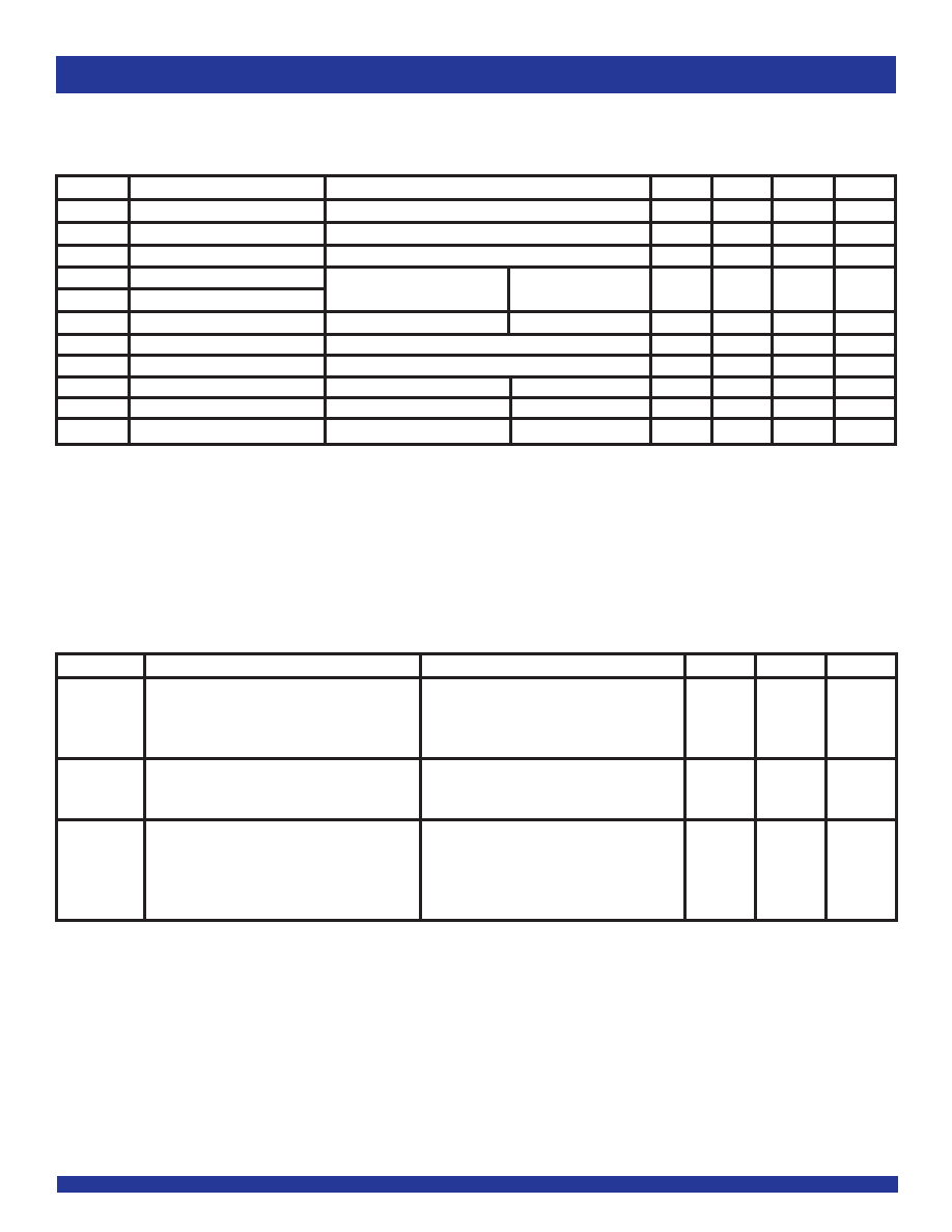
Symbol
Parameter
Test Conditions
Min.
Typ.(1)
Max.
Unit
VIH
Input HIGH Level
Guaranteed Logic HIGH Level
2
—
V
VIL
Input LOW Level
Guaranteed Logic LOW Level
—
0.8
V
VT
Input Hysteresis
VTLH - VTHL for all inputs
—
0.2
—
V
IIH
Input HIGH Current
VCC = Max.
0
≤ VIN ≤ VCC
——
±5A
IIL
Input LOW Current
IOZ
Off-State Output Current (Hi-Z)
VCC = Max
0
≤ VIN ≤ VCC
——
±5A
IOR
Current Drive
VCC = Max., VOUT = 2.0V(2)
50
—
mA
VIC
Input Clamp Voltage
VCC = Min, IIN = -18mA , TA = 25°C(2)
—
–0.7
–1.2
V
VOH
Output HIGH Voltage
VCC = Min.
IOH = -15mA
2.4
—
V
VOL
OutputLOWVoltage
VCC = Min.
IOL = 12mA
—
0.5
V
ROUT(3)
OutputResistance
VCC = Min.
IOH = 12mA
15
21
40
DC ELECTRICAL CHARACTERISTICS OVER OPERATING RANGE
FollowingConditionsApplyUnlessOtherwiseSpecified:
Industrial: TA = –40°C to +85°C, VCC = 5.0V ±5%
NOTES:
1. Typical values are at VCC = 5.0V, TA = 25°C.
2. This parameter is measured at characterization but not tested.
3. ROUT changed on March 8, 2002. See rear page for more information.
POWER SUPPLY CHARACTERISTICS
Following Conditions Apply Unless Otherwise Specified:
Industrial: TA = -40°C to +85°C, VCC = 5.0V ± 5%
Symbol
Parameter
TestConditions(1)
Min.
Max.
Unit
ICC
Quiescent Power Supply Current
VCC = Max.
—
1.5
mA
freq = 0
0V
≤ VIN ≤ 0.2V or
VCC - 0.2V
≤ VIN ≤ Vcc
ICC
Supply Current per Input TTL Inputs HIGH
VCC = Max.
—
2
mA
VIN = 3.4V(2)
freq = 0
ICCD
Supply Current per Input per MHz
VCC = Max.
—
0.25
mA/MHz
OutputsOpenandEnabled
OneBitToggling
50% Duty Cycle
Other inputs at GND or Vcc(3,4)
NOTES:
1. For conditions shown as Min. or Max., use the appropriate values specified under DC Electrical Characteristics.
2. Per TLL driven input (VIN = 3.4V).
3. For flip-flops, ICCD is measured by switching one of the data input pins so that the output changes every clock cycle. This is a measurement of device power consumption
only and does not include power to drive load capacitance or tester capacitance.
4. IC = IQUIESCENT + IINPUTS + IDYNAMIC
IC = ICC +
ICC DHNT + ICCD (fCP/2 + fiNi)
ICC = Quiescent Current
ICC = Power Supply Current for a TTL High Input (VIN = 3.4V)
DH = Duty Cycle for TTL Inputs High
NT = Number of TTL Inputs at DH
ICCD = Dynamic Current Caused by an Output Transition Pair (HLH or LHL)
fCP = Clock Frequency for Register Devices (Zero for Non-Register Devices)
fi = Input Frequency
Ni = Number of Inputs at fi
All currents are in milliamps and all frequencies are in megahertz.
相关PDF资料 |
PDF描述 |
|---|---|
| IDTQS74FCT2573TSO | FCT SERIES, 8-BIT DRIVER, TRUE OUTPUT, PDSO20 |
| IDTQS74FCT2573TQ | FCT SERIES, 8-BIT DRIVER, TRUE OUTPUT, PDSO20 |
| IDTQS74FCT2573ATQ | FCT SERIES, 8-BIT DRIVER, TRUE OUTPUT, PDSO20 |
| IDTQS74FCT2574TQ8 | FCT SERIES, 8-BIT DRIVER, TRUE OUTPUT, PDSO20 |
| IDTQS74FCT2574CTQ | FCT SERIES, 8-BIT DRIVER, TRUE OUTPUT, PDSO20 |
相关代理商/技术参数 |
参数描述 |
|---|---|
| IDTQS74FCT2573TQ | 制造商:未知厂家 制造商全称:未知厂家 功能描述:LATCH|SINGLE|8-BIT|FCT/PCT-CMOS|SOP|20PIN|PLASTIC |
| IDTQS74FCT2573TSO | 制造商:未知厂家 制造商全称:未知厂家 功能描述:8-Bit D-Type Latch |
| IDTQS74FCT2574ATQ | 制造商:未知厂家 制造商全称:未知厂家 功能描述:Buffer/Driver |
| IDTQS74FCT2574ATSO | 制造商:未知厂家 制造商全称:未知厂家 功能描述:Buffer/Driver |
| IDTQS74FCT2574CTQ | 制造商:未知厂家 制造商全称:未知厂家 功能描述:Buffer/Driver |
发布紧急采购,3分钟左右您将得到回复。