- 您现在的位置:买卖IC网 > PDF目录67718 > IL4217-X019 (VISHAY SEMICONDUCTORS) 1 CHANNEL TRIAC OUTPUT OPTOCOUPLER PDF资料下载
参数资料
| 型号: | IL4217-X019 |
| 厂商: | VISHAY SEMICONDUCTORS |
| 元件分类: | 光电耦合器 |
| 英文描述: | 1 CHANNEL TRIAC OUTPUT OPTOCOUPLER |
| 封装: | ROHS COMPLIANT, SMD, 6 PIN |
| 文件页数: | 7/13页 |
| 文件大小: | 241K |
| 代理商: | IL4217-X019 |
Document Number: 83630
For technical questions, contact: optocoupleranswers@vishay.com
www.vishay.com
Rev. 1.6, 20-Oct-10
3
IL4216, IL4217, IL4218
Optocoupler, Phototriac Output,
High dV/dt, Low Input Current
Vishay Semiconductors
Note
Minimum and maximum values are testing requirements. Typical values are characteristics of the device and are the result of engineering
evaluation. Typical values are for information only and are not part of the testing requirements.
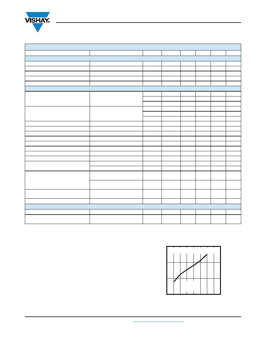
POWER FACTOR CONSIDERATIONS
A snubber is not needed to eliminate false operation of the
TRIAC driver because of the IL4216, IL4217, IL4218 high
static and commutating dV/dt with loads between 1 and 0.8
power factors. When inductive loads with power factors less
than 0.8 are being driven, include a RC snubber or a single
capacitor directly across the device to damp the peak
commutating dV/dt spike. Normally a commutating dV/dt
causes a turning-off device to stay on due to the stored
energy remaining in the turning-off device.
Fig. 1 - Shunt Capacitance vs. Load Current vs. Power Factor
ELECTRICAL CHARACTERISTICS (Tamb = 25 °C, unless otherwise specified)
PARAMETER
TEST CONDITION
PART
SYMBOL
MIN.
TYP.
MAX.
UNIT
INPUT
Forward voltage
IF = 20 mA
VF
1.3
1.5
V
Breakdown voltage
IR = 10 μA
VBR
630
V
Reverse current
VR = 6 V
IR
0.1
10
μA
Input capacitance
VF = 0 V, f = 1 MHz
CIN
40
pF
Thermal resistance, junction to lead
RthjI
750
°C/W
OUTPUT
Repetitive peak off-state voltage
IDRM = 100 μA
IL4216
VDRM
600
650
V
IL4217
VDRM
700
750
V
IL4218
VDRM
800
850
V
Off-state voltage
ID(RMS) = 70 μA
IL4216
VD(RMS)
424
460
V
IL4217
VD(RMS)
484
536
V
IL4218
VD(RMS)
565
613
V
Off-state current
VD = 600 V, Tamb = 100 °C
ID(RMS)
10
100
μA
Reverse current
VR = 600 V, Tamb = 25 °C
IRMS
10
100
μA
On-state voltage
IT = 300 mA
VTM
1.7
3
V
On-state current
PF = 1, VT(RMS) = 1.7 V
ITM
300
mA
Surge (non-repetitive, on-state current)
f = 50 Hz
ITSM
3A
Holding current
VT = 3 V
IH
65
200
μA
Latching current
VT = 2.2 V
IL
500
μA
LED trigger current
VAK = 5 V
IFT
0.7
mA
Critical rate of rise of off-state voltage
VD = 0.67 VDRM, Tamb = 25 °C
dV/dtcr
10 000
V/μs
VD = 0.67 VDRM, Tamb = 80 °C
dV/dtcr
5000
V/μs
Critical rate of rise of voltage at current
commutation
VD = 230 VRMS,
ID = 300 mARMS, TJ = 25 °C
dV/dtcrq
8V/μs
VD = 230 VRMS,
ID = 300 mARMS, TJ = 85 °C
dV/dtcrq
7V/μs
Critical rate of rise of on-state current
commutation
VD = 230 VRMS,
ID = 300 mARMS, TJ = 25 °C
dI/dtcrq
12
A/ms
Thermal resistance, junction to lead
RthjI
150
°C/W
COUPLER
Capacitance (input to output)
f = 1 MHz, VIO = 0 V
CIO
0.8
pF
Critical rate of rise of coupled
input to output voltage
IT = 0, VRM = VDM = 300 VAC
dV(IO)/dt
5000
1
mA
iil4116_07
400
350
300
250
200
150
100
50
0
I - Load Current (mA)
C
S
-Shunt
Capacitance
(F)
L
0.001
0.01
0.1
1
C (F) = 0.0032 (F) x 10 ^ (0.0066 I
L (mA))
S
P
F = 0.3
I
F = 2.0 mA
相关PDF资料 |
PDF描述 |
|---|---|
| IL4218-X007 | 1 CHANNEL TRIAC OUTPUT OPTOCOUPLER |
| IL440-4 | 1 CHANNEL TRIAC OUTPUT OPTOCOUPLER |
| IL440-5X016 | 1 CHANNEL TRIAC OUTPUT OPTOCOUPLER |
| IL440-6X007 | 1 CHANNEL TRIAC OUTPUT OPTOCOUPLER |
| IL440-4-X017 | 1 CHANNEL TRIAC OUTPUT OPTOCOUPLER |
相关代理商/技术参数 |
参数描述 |
|---|---|
| IL4218 | 功能描述:三极与 SCR 输出光电耦合器 Phototriac Output Very Low Input Curr RoHS:否 制造商:Vishay Semiconductors 输出设备:PhotoTriac 每芯片的通道数量: 绝缘电压:3750 Vrms 正向电流:10 mA 正向电压:1.2 V 最大触发电流:10 mA 关断状态下输出电压-VDRM:600 V 最大连续输出电流: 零交叉电路: 封装:Reel |
| IL4218 | 制造商:Vishay Semiconductors 功能描述:Optocoupler |
| IL42181002 | 制造商:Vishay Angstrohm 功能描述:OPTOCOUPLER PHOTOTRIAC OUTPUT HIGH DV/DT VERY LOW INPUT CURRENT |
| IL4218-2029 | 制造商:Vishay Angstrohm 功能描述:SPECIAL TEST/MARK |
| IL4218-X001 | 功能描述:三极与 SCR 输出光电耦合器 Phototriac Output, Low Input Current RoHS:否 制造商:Vishay Semiconductors 输出设备:PhotoTriac 每芯片的通道数量: 绝缘电压:3750 Vrms 正向电流:10 mA 正向电压:1.2 V 最大触发电流:10 mA 关断状态下输出电压-VDRM:600 V 最大连续输出电流: 零交叉电路: 封装:Reel |
发布紧急采购,3分钟左右您将得到回复。