- 您现在的位置:买卖IC网 > PDF目录61113 > ILD615-2 (VISHAY INTERTECHNOLOGY INC) 2 CHANNEL TRANSISTOR OUTPUT OPTOCOUPLER PDF资料下载
参数资料
| 型号: | ILD615-2 |
| 厂商: | VISHAY INTERTECHNOLOGY INC |
| 元件分类: | 光电耦合器 |
| 英文描述: | 2 CHANNEL TRANSISTOR OUTPUT OPTOCOUPLER |
| 文件页数: | 1/5页 |
| 文件大小: | 419K |
| 代理商: | ILD615-2 |
Document Number: 83652
www.vishay.com
Revision 17-August-01
2–193
DUAL CHANNEL
ILD615
QUAD CHANNEL
ILQ615
Phototransistor Optocoupler
FEATURES
Identical Channel to Channel Footprint
Current Transfer Ratio (CTR) Range, IF=10 mA
ILD/Q615-1: 40–80% Min.
ILD/Q615-2: 63–125% Min.
ILD/Q615-3: 100–200% Min.
ILD/Q615-4: 160–320% Min.
Guaranteed CTR, IF=1.0 mA
ILD/Q615-1: 13% Min.
ILD/Q615-2: 22% Min.
ILD/Q615-3: 34% Min.
ILD/Q615-4: 56% Min.
High Collector-Emitter Voltage, BVCEO=70 V
Dual and Quad Packages Feature:
– Reduced Board Space
– Lower Pin and Parts Count
– Better Channel to Channel CTR Match
– Improved Common Mode Rejection
Field-Effect Stable by TRIOS (TRansparent IOn
Shield)
Isolation Test Voltage from Double Molded
Package, 5300 VRMS
UL Approval #E52744
VDE #0884 Available with Option 1
Maximum Ratings (Each Channel)
Emitter
Reverse Voltage .............................................. 6.0 V
Forward Current ........................................... 60 mA
Surge Current ................................................. 1.5 A
Power Dissipation ...................................... 100 mW
Derate Linearly from 25
°C ................... 1.33 mW/°C
Detector
Collector-Emitter Reverse Voltage .................. 70 V
Emitter-Collector Reverse Voltage ................. 7.0 V
Collector Current .......................................... 50 mA
Collector Current (t <1.0 ms) ...................... 100 mA
Power Dissipation ...................................... 150 mW
Derate Linearly from 25
°C..................... 2.0 mW/°C
Package
Storage Temperature.................... –55
°C to +150°C
Operating Temperature ............... –55
°C to +100°C
Junction Temperature.................................... 100
°C
Soldering Temperature
(2.0 mm distance from case bottom) ........ 260
°C
Package Power Dissipation, ILD615.......... 400 mW
Derate Linearly from 25
°C.................. 5.33 mW/°C
Package Power Dissipation, ILQ615 ......... 500 mW
Derate Linearly from 25
°C................. 6.67 mW/°C
Isolation Test Voltage (t=1.0 sec.) .......... 5300 VRMS
Creepage .................................................
≥7.0 mm
Clearance.................................................
≥7.0 mm
Isolation Resistance
VIO=500 V, TA=25°C .............................. ≥10
12
VIO=500 V, TA=100°C ............................ ≥10
11
V
DE
DESCRIPTION
The ILD/Q615 are multi-channel phototransistor optocouplers that use GaAs
IRLED emitters and high gain NPN phototransistors. These devices are con-
structed using over/under leadframe optical coupling and double molded
insulation technology resulting a Withstand Test Voltage of 7500 VACPEAK
and a Working Voltage of 1700 VRMS.
The binned min./max. and linear CTR characteristics combined with the
TRIOS (TRansparent IOn Shield) eld-effect process make these devices
well suited for DC or AC voltage detection. Eliminating the phototransistor
base connection provides added electrical noise immunity from the tran-
sients found in many industrial control environments.
Because of guaranteed maximum non-saturated and saturated switching
characteristics, the ILD/Q615 can be used in medium speed data I/O and
control systems. The binned min./max. CTR specication allow easy worst
case interface calculations for both level detection and switching applica-
tions. Interfacing with a CMOS logic is enhanced by the guaranteed CTR at
IF=1.0 mA.
See Appnote 45, “How to Use Optocoupler Normalized Curves”.
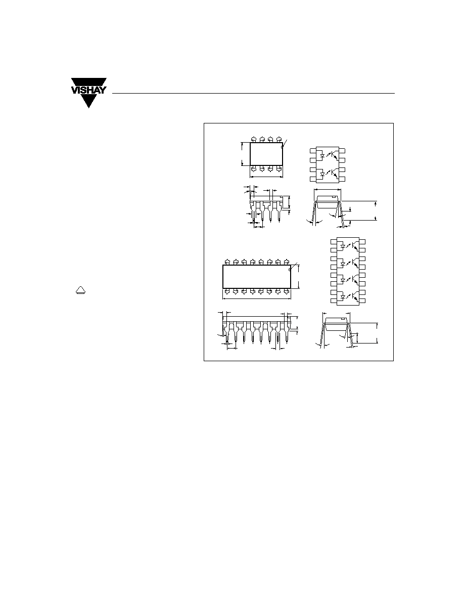
pin
one ID
.255 (6.48)
.268 (6.81)
.379 (9.63)
.390 (9.91)
.030 (0.76)
.045 (1.14)
4
° typ.
.100 (2.54) typ.
10
°
3
°–9°
.300 (7.62)
typ.
.018 (.46)
.022 (.56)
.008 (.20)
.012 (.30)
.110 (2.79)
.130 (3.30)
.150 (3.81)
.020 (.51 )
.035 (.89 )
.230(5.84)
.250(6.35)
4
3
2
1
.031 (0.79)
.050 (1.27)
5
6
78
1
2
3
4
8
7
6
5
Collector
Emitter
Collector
Emitter
Anode
Cathode
Anode
Cathode
Collector
Emitter
Collector
Emitter
Collector
Emitter
Collector
Emitter
Anode
Cathode
Anode
Cathode
Anode
Cathode
Anode
Cathode
1
2
3
4
5
6
7
8
16
15
14
13
12
11
10
9
.255 (6.48)
.265 (6.81)
.779 (19.77 )
.790 (20.07)
.030 (.76)
.045 (1.14)
4
°
.100 (2.54)typ.
10
°
typ.
3
°–9°
.018 (.46)
.022 (.56)
.008 (.20)
.012 (.30)
.110 (2.79)
.130 (3.30)
pin
one ID
.130 (3.30)
.150 (3.81)
.020(.51)
.035 (.89)
8
7
6
5
4
3
2
1
9
10
11 12
13
14
15
16
.031(.79)
.300 (7.62)
typ.
.230 (5.84)
.250 (6.35)
.050 (1.27)
Dimensions in inches (mm)
相关PDF资料 |
PDF描述 |
|---|---|
| ILD615-4 | 2 CHANNEL TRANSISTOR OUTPUT OPTOCOUPLER |
| ILD615-1 | 2 CHANNEL TRANSISTOR OUTPUT OPTOCOUPLER |
| ILQ615-2 | 4 CHANNEL TRANSISTOR OUTPUT OPTOCOUPLER |
| ILQ615-3-X016 | 4 CHANNEL TRANSISTOR OUTPUT OPTOCOUPLER |
| ILQ615-1-X007 | 4 CHANNEL TRANSISTOR OUTPUT OPTOCOUPLER |
相关代理商/技术参数 |
参数描述 |
|---|---|
| ILD615-2 | 制造商:Vishay Semiconductors 功能描述:Optocoupler |
| ILD615-2X001 | 功能描述:晶体管输出光电耦合器 DIP-8 CPL DUAL 63-125% CTR VD RoHS:否 制造商:Vishay Semiconductors 输入类型:DC 最大集电极/发射极电压:70 V 最大集电极/发射极饱和电压:0.4 V 绝缘电压:5300 Vrms 电流传递比:100 % to 200 % 最大正向二极管电压:1.65 V 最大输入二极管电流:60 mA 最大集电极电流:100 mA 最大功率耗散:100 mW 最大工作温度:+ 110 C 最小工作温度:- 55 C 封装 / 箱体:DIP-4 封装:Bulk |
| ILD615-2X006 | 制造商:VISHAY 制造商全称:Vishay Siliconix 功能描述:Optocoupler, Phototransistor Output (Dual, Quad Channel) |
| ILD615-2X009 | 功能描述:晶体管输出光电耦合器 Phototransistor Out Dual CTR > 63-125% RoHS:否 制造商:Vishay Semiconductors 输入类型:DC 最大集电极/发射极电压:70 V 最大集电极/发射极饱和电压:0.4 V 绝缘电压:5300 Vrms 电流传递比:100 % to 200 % 最大正向二极管电压:1.65 V 最大输入二极管电流:60 mA 最大集电极电流:100 mA 最大功率耗散:100 mW 最大工作温度:+ 110 C 最小工作温度:- 55 C 封装 / 箱体:DIP-4 封装:Bulk |
| ILD615-2X009T | 功能描述:晶体管输出光电耦合器 SMD-8 CPL DUAL 63-125% CTR -E RoHS:否 制造商:Vishay Semiconductors 输入类型:DC 最大集电极/发射极电压:70 V 最大集电极/发射极饱和电压:0.4 V 绝缘电压:5300 Vrms 电流传递比:100 % to 200 % 最大正向二极管电压:1.65 V 最大输入二极管电流:60 mA 最大集电极电流:100 mA 最大功率耗散:100 mW 最大工作温度:+ 110 C 最小工作温度:- 55 C 封装 / 箱体:DIP-4 封装:Bulk |
发布紧急采购,3分钟左右您将得到回复。