- 您现在的位置:买卖IC网 > PDF目录67719 > IMIC9714JY (CYPRESS SEMICONDUCTOR CORP) PROC SPECIFIC CLOCK GENERATOR, PDSO28 PDF资料下载
参数资料
| 型号: | IMIC9714JY |
| 厂商: | CYPRESS SEMICONDUCTOR CORP |
| 元件分类: | 时钟产生/分配 |
| 英文描述: | PROC SPECIFIC CLOCK GENERATOR, PDSO28 |
| 封装: | SSOP-28 |
| 文件页数: | 2/12页 |
| 文件大小: | 109K |
| 代理商: | IMIC9714JY |
C9714J
100 MHz Clock Generator with SSCG and Power Management for Mobile Application
Preliminary
INTERNATIONAL MICROCIRCUITS, INC. 525 LOS COCHES ST.
Rev. 1.0
4/28/2000
MILPITAS, CA 95035 TEL: 408-263-6300 ext. 275 FAX 408-263-6571
Page 10 of 12
Suggested Oscillator Crystal Parameters
Characteristic
Symbol
Min
Typ
Max
Units
Conditions
Frequency
Fo
14.17
14.31818
14.46
MHz
Tolerance
TC
-
+/-100
PPM
Note 1
Frequency Stability
TS
-
+/- 100
PPM
Stability (TA -10 to +60C) Note 1
Operating Mode
-
Parallel Resonant, Note 1
Load Capacitance
CXTAL
-
20
-
pF
The crystal’s rated load. Note 1
Effective Series
Resistance (ESR)
RESR
-
40
-
Ohms
Note 2
Note1:
For best performance and accurate frequencies from this device, It is recommended but not mandatory that the chosen
crystal meets or exceeds these specifications
Note 2: Larger values may cause this device to exibit oscillator startup problems
To obtain the maximum accuracy, the total circuit loading capacitance should be equal to CXTAL. This loading capacitance is the
effective capacitance across the crystal pins and includes the clock generating device pin capacitance (CFTG), any circuit trace
capacitance (CPCB), and any onboard discrete load capacitance (CDISC).
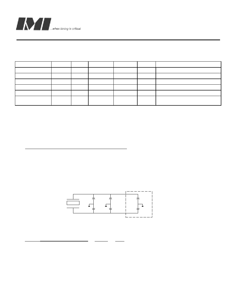
The following formula and schematic illustrates the application of the loading specification of a crystal (CXTAL)for a design.
CL = (CXINPCB + CXINFTG + CXINDISC) X (CXOUTPCB + CXOUTFTG + CXOUTDISC)
(CXINPCB + CXINFTG + CXINDISC) + (CXOUTPCB + CXOUTFTG + COUTDISC)
Where:
CXTAL
= the load rating of the crystal
CXOUTFTG
= the clock generators XIN pin effective device internal capacitance to ground
CXOUTFTG
= the clock generators XOUT pin effective device internal capacitance to ground
CXINPCB
= the effective capacitance to ground of the crystal to device PCB trace
CXOUTPCB
= the effective capacitance to ground of the crystal to device PCB trace
CXINDISC
= any discrete capacitance that is placed between the XIN pin and ground
CXOUTDISC = any discrete capacitance that is placed between the XOUT pin and ground
C
XINPCB
C
XOUTPCB
C
XOUTDISC
C
XINDISC
C
XINFTG
C
XOUTFTG
XIN
XOUT
Clock Generator
As an example, and using this formula for this datasheet’s device, a design that has no discrete loading capacitors (CDISC) and each
of the crystal to device PCB traces has a capacitance (CPCB) to ground of 4pF (typical value) would calculate as:
CL = (4pF + 36pF + 0pF) X (4pF + 36pF + 0pF)
= 40 X 40
= 1600
= 20pF
(4pF + 36pF + 0pF) + (4pF + 36pF + 0pF)
40 + 40
80
Therefore to obtain output frequencies that are as close to this data sheets specified values as possible, in this design example, you
should specify a parallel cut crystal that is designed to work into a load of 20pF
相关PDF资料 |
PDF描述 |
|---|---|
| IMIC9716-ITB | PROC SPECIFIC CLOCK GENERATOR, PDSO28 |
| IMIC9717CYB | PROC SPECIFIC CLOCK GENERATOR, PDSO28 |
| IMIC9717CTB | PROC SPECIFIC CLOCK GENERATOR, PDSO28 |
| IMIC9806AYB | PROC SPECIFIC CLOCK GENERATOR, PDSO48 |
| IMIC9806CY | PROC SPECIFIC CLOCK GENERATOR, PDSO48 |
相关代理商/技术参数 |
参数描述 |
|---|---|
| IMIC9716J | 制造商:未知厂家 制造商全称:未知厂家 功能描述:100 MHz Clock Generator with SSCG and Power Management for Mobile Application |
| IMIC9716JT | 制造商:未知厂家 制造商全称:未知厂家 功能描述:100 MHz Clock Generator with SSCG and Power Management for Mobile Application |
| IMIC9716JY | 制造商:未知厂家 制造商全称:未知厂家 功能描述:100 MHz Clock Generator with SSCG and Power Management for Mobile Application |
| IMIC9717 | 制造商:未知厂家 制造商全称:未知厂家 功能描述:100 MHz Clock Generator with SSCG and Power Management for Mobile Application |
| IMIC9717CTB | 制造商:未知厂家 制造商全称:未知厂家 功能描述:100 MHz Clock Generator with SSCG and Power Management for Mobile Application |
发布紧急采购,3分钟左右您将得到回复。