- 您现在的位置:买卖IC网 > PDF目录67719 > IMIC9717CTB PROC SPECIFIC CLOCK GENERATOR, PDSO28 PDF资料下载
参数资料
| 型号: | IMIC9717CTB |
| 元件分类: | 时钟产生/分配 |
| 英文描述: | PROC SPECIFIC CLOCK GENERATOR, PDSO28 |
| 文件页数: | 6/13页 |
| 文件大小: | 129K |
| 代理商: | IMIC9717CTB |
C9717
100 MHz Clock Generator with SSCG and Power Management for Mobile
Application
Approved Product
INTERNATIONAL MICROCIRCUITS, INC. 525 LOS COCHES ST.
Rev. 1.2
6/25/1999
MILPITAS, CA 95035 TEL: 408-263-6300 ext. 275 FAX 408-263-6571
Page 2 of 13
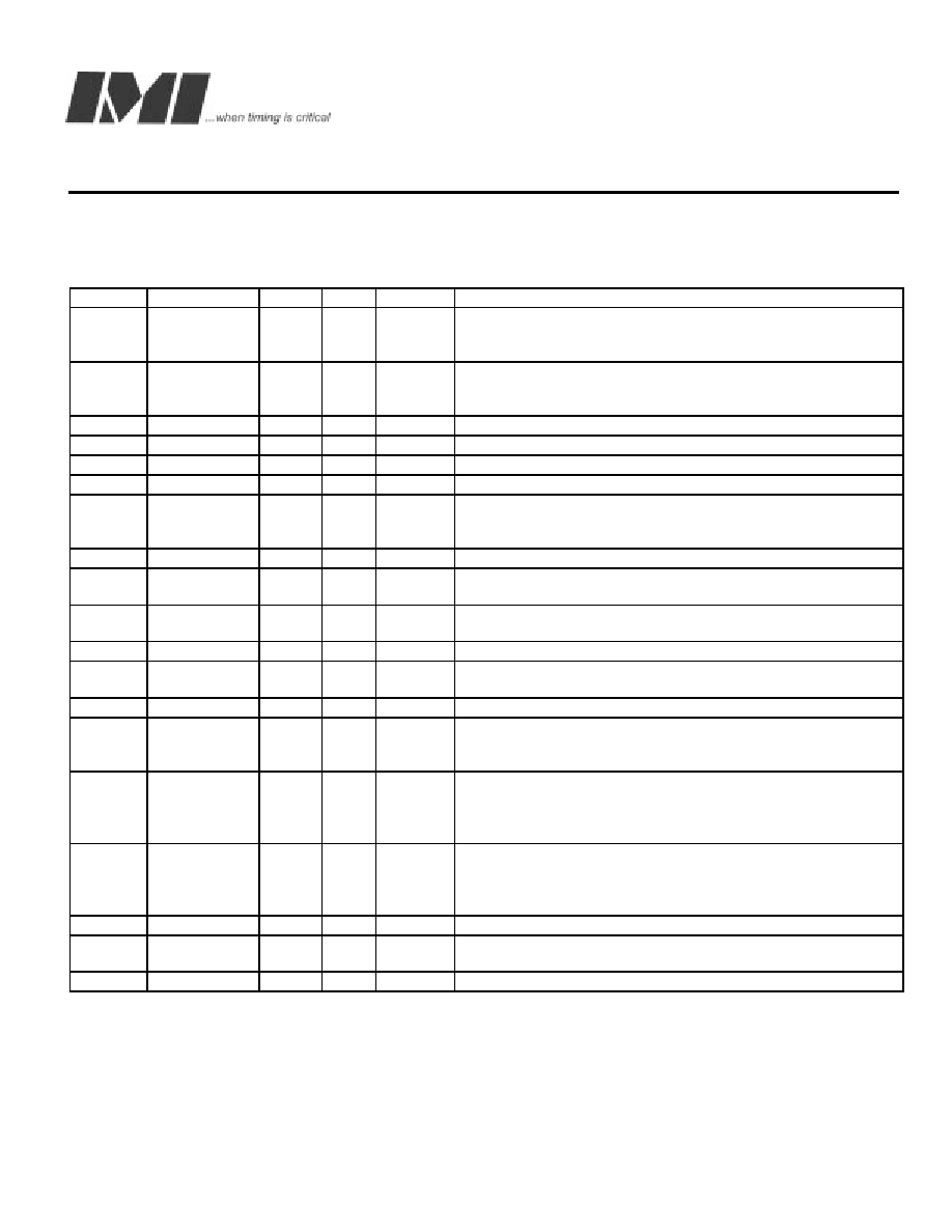
Pin Description
PIN No.
Pin Name
PWR
I/O
TYPE
Description
2
XIN
VDD
I
XTAL4
On-chip reference oscillator input pin. Requires either an
external parallel resonant crystal (nominally 14.318 MHz) or
externally generated reference signal
3
XOUT
VDD
O
XTAL4
O-chip reference oscillator output pin. Drives an external
parallel resonant crystal (14.318 MHz) when an externally
generated reference signal is used.
19
VDD
-
P
PWR
3.3 volt power supply for core logic.
23, 24
CPU (1,2)
VDDC
O
C100S
Clock outputs. CPU frequency table specified on page 1.
17
PD#
-
I
INP3U
Powers down device when LOW
18
CS#
-
I
INP3U
When signal is LOW, stops CPU clocks in low state.
16
SEL100/66#
-
I
INP3
Frequency select input pins. See frequency select table on
page 1. NO INTERNAL PULLUP RESISTOR IS PROVIDED
BY DEVICE
25
VDDC
-
P
PWR
2.5V power for CPU and Host clock outputs.
4
PCI_F
VDDP
O
P100S
Free running PCI clock 3.3V. Does not stop when PS# is at a
logic LOW level
5,6,9,
10,11
PCI(1:5)
VDDP
O
P100S
PCI output clocks. See frequency table of page 1.
20
PS#
-
I
INP3U
When signal is LOW, stops all PCI clocks in low state.
8
VDDP
-
P
PWR
3.3 Volt power supply pins for free running PCI clock output
buffer.
13
48M
VDDF
O
U48
Fixed 48 MHz clock.
14
48-24M/TS#
VDDF
I/O
U48BU
Power up selectable 48 or 24 MHz clock. If strapped LOW at
powerup causes the devices outputs to be tri-stated until the
next power up sequence occurs.
26
REF1/SS#
VDDR
I/O
U48BU
At power up this pin determines if the device’s spread
spectrum modulation feature is enabled or disabled. After
power up this pin becomes a reference clock output. A 0 (logic
low) enables SSCG and a 1 (logic high) disables SSCG.
27
REF2/SEL48
#
VDDR
I/O
U48BU
At power up this pin determine the frequency of the clock at pin
14. If it is LOW, the clock will be 48 MHz, if HIGH the clock will
be 24 MHz. After power up this pin will become a reference
clock output.
12
VDDF
-
P
PWR
Power for fixed clock output buffer.
1, 7, 15,
21, 22
VSS
-
P
PWR
Ground pins for device.
28
VDDR
-
P
PWR
Power for Reference Oscillator output buffer.
Notes
1.
INP3U pins have internal pullup resistors that will guarantee to a logic 1 (high) level if no connection is made to the
device’s pin. INP3 pins do not contain this function and must be electrically connected to VDD or VSS by external
circuitry to ensure a valid logic 1 or 0 is sensed.
相关PDF资料 |
PDF描述 |
|---|---|
| IMIC9806AYB | PROC SPECIFIC CLOCK GENERATOR, PDSO48 |
| IMIC9806CY | PROC SPECIFIC CLOCK GENERATOR, PDSO48 |
| IMIC9806IAT | PROC SPECIFIC CLOCK GENERATOR, PDSO48 |
| IMIFS782BZBT | 82 MHz, OTHER CLOCK GENERATOR, PDSO8 |
| IMIFS784BZBT | 82 MHz, OTHER CLOCK GENERATOR, PDSO8 |
相关代理商/技术参数 |
参数描述 |
|---|---|
| IMIC9717CYB | 制造商:未知厂家 制造商全称:未知厂家 功能描述:100 MHz Clock Generator with SSCG and Power Management for Mobile Application |
| IMIC9806JBT | 制造商:Cypress Semiconductor 功能描述:Development Tools, Notebook, Intel Piii /Celeron 制造商:Rochester Electronics LLC 功能描述:- Bulk |
| IMIC9812DYBD | 制造商:IMI 功能描述: |
| IMIC9827H | 制造商:未知厂家 制造商全称:未知厂家 功能描述:Clocks and Buffers |
| IMIC9827JT | 制造商:Rochester Electronics LLC 功能描述:TIMING DEVICE - Tape and Reel |
发布紧急采购,3分钟左右您将得到回复。