- 您现在的位置:买卖IC网 > PDF目录67719 > IMIC9717CYB PROC SPECIFIC CLOCK GENERATOR, PDSO28 PDF资料下载
参数资料
| 型号: | IMIC9717CYB |
| 元件分类: | 时钟产生/分配 |
| 英文描述: | PROC SPECIFIC CLOCK GENERATOR, PDSO28 |
| 文件页数: | 12/13页 |
| 文件大小: | 129K |
| 代理商: | IMIC9717CYB |
C9717
100 MHz Clock Generator with SSCG and Power Management for Mobile
Application
Approved Product
INTERNATIONAL MICROCIRCUITS, INC. 525 LOS COCHES ST.
Rev. 1.2
6/25/1999
MILPITAS, CA 95035 TEL: 408-263-6300 ext. 275 FAX 408-263-6571
Page 8 of 13
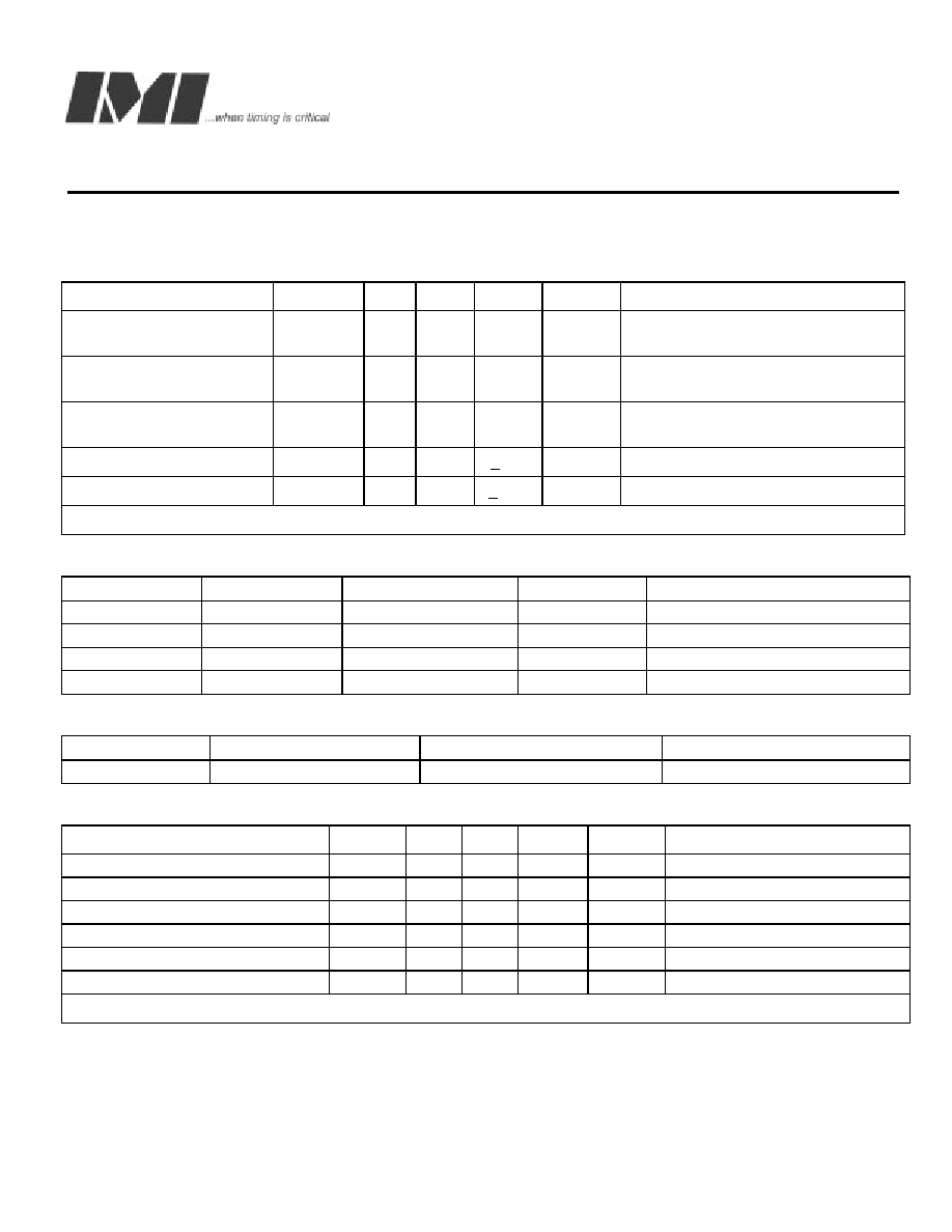
AC Parameters
Characteristic
Symbol
Min
Typ
Max
Units
Conditions
Output Duty Cycle
-
45
50
55
%
CPU and CPU/2 = Measured at 1.25V
all others measured at 1.50V
CPU to PCI Offset
tOFF
1
-
4
ns
CPU = 20 pF load Measured at 1.25V
PCI = 30 pF load Measure at 1.50V
Buffer out Skew All CPU
and PCI Buffer Outputs
tSKEW
-
250
ps
CPU = 20 pF load Measured at 1.25V
PCI = 30 pF Load Measured at 1.5V
Period Adjacent Cycles
P
-
+250
ps
CPU and CPU/2
Period Adjacent Cycles
P
-
+ 500
pS
PCI Only
VDD = VDDF = VDDP =VDDR =3.3V
±5%, VDDC = 2.5V ±5%,, TA = 0C to +70C
AC Skew Requirements
Characteristic
Bank Skew
Cycle to Cycle Jitters
VDD
Skew, Jitters Measure Point
CPU
175pS
+/- 250pS
2.5V
1.25V
48 MHz
n/a
+/- 500pS
3.3V
1.5V
PCI, PCI_F
500pS
+/- 500pS
3.3V
1.5V
Ref
n/a
+/- 500pS
3.3V
1.5V
Offset Requirements
Characteristic
Bank Offset
Measurement Loads (lumped)
Measure Points
CPU to PCI, PCI-5
1.5-4.0nS CPU leads
CPU @ 20pF, PCI @ 30 pF
CPU @ 1.25V, PCI @ 1.5V
DC Buffer Characteristics for CPU Outputs
Characteristic
Symbol
Min
Typ
Max
Units
Conditions
Pull-Up Current Min
IOHmin
-82
-
mA
Vout = 1.0 V
Pull-Up Current Max
IOHmax
-67
mA
Vout = 2.375 V
Pull-Down Current Min
IOLmin
81
-
mA
Vout = 1.2 V
Pull-Down Current Max
IOLmax
-
60
mA
Vout = 0.3 V
Rise Time Between 0.4 V and 2.4 V
TR
0.4
-
1.6
nS
20 pF Load
Fall Time Between 0.4 V and 2.4 V
TF
0.5
-
1.6
nS
20 pF Load
VDD = VDDF = VDDP = VDDR =3.3V
±5%, VDDC = 2.5V ±5%,, TA = 0C to +70C
相关PDF资料 |
PDF描述 |
|---|---|
| IMIC9717CTB | PROC SPECIFIC CLOCK GENERATOR, PDSO28 |
| IMIC9806AYB | PROC SPECIFIC CLOCK GENERATOR, PDSO48 |
| IMIC9806CY | PROC SPECIFIC CLOCK GENERATOR, PDSO48 |
| IMIC9806IAT | PROC SPECIFIC CLOCK GENERATOR, PDSO48 |
| IMIFS782BZBT | 82 MHz, OTHER CLOCK GENERATOR, PDSO8 |
相关代理商/技术参数 |
参数描述 |
|---|---|
| IMIC9806JBT | 制造商:Cypress Semiconductor 功能描述:Development Tools, Notebook, Intel Piii /Celeron 制造商:Rochester Electronics LLC 功能描述:- Bulk |
| IMIC9812DYBD | 制造商:IMI 功能描述: |
| IMIC9827H | 制造商:未知厂家 制造商全称:未知厂家 功能描述:Clocks and Buffers |
| IMIC9827JT | 制造商:Rochester Electronics LLC 功能描述:TIMING DEVICE - Tape and Reel |
| IMIC9827JTT | 制造商:Rochester Electronics LLC 功能描述:TIMING DEVICE - Bulk |
发布紧急采购,3分钟左右您将得到回复。