- 您现在的位置:买卖IC网 > PDF目录378630 > IN74HC4052 (INTEGRAL JOINT STOCK COMPANY) Octal Edge-Triggered D-Type Flip-Flops With 3-State Outputs 20-TSSOP -40 to 85 PDF资料下载
参数资料
| 型号: | IN74HC4052 |
| 厂商: | INTEGRAL JOINT STOCK COMPANY |
| 英文描述: | Octal Edge-Triggered D-Type Flip-Flops With 3-State Outputs 20-TSSOP -40 to 85 |
| 中文描述: | 模拟多路复用器/解复用器 |
| 文件页数: | 2/8页 |
| 文件大小: | 152K |
| 代理商: | IN74HC4052 |
IN74HC4052
500
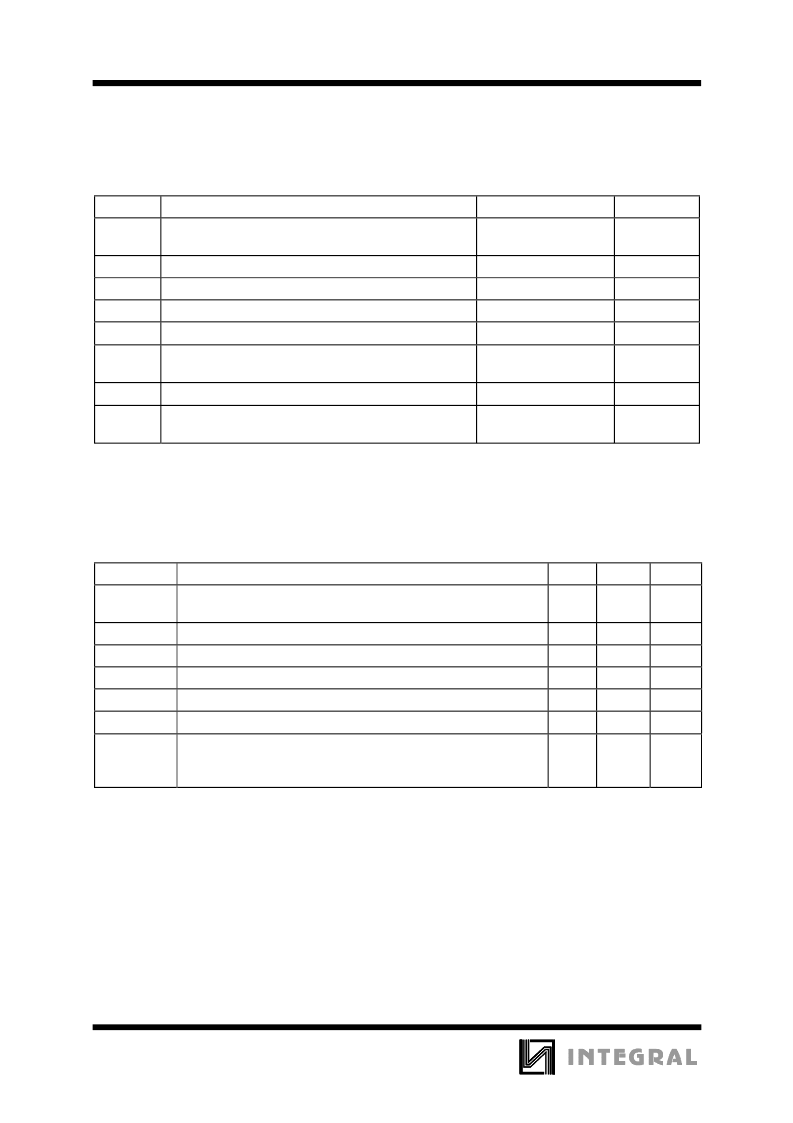
MAXIMUM RATINGS
*
Symbol
Parameter
Value
Unit
V
CC
Positive DC Supply Voltage (Referenced to GND)
(Referenced to V
EE
)
Negative DC Supply Voltage (Referenced to GND)
-0.5 to +7.0
-0.5 to +14.0
V
V
EE
V
IS
V
IN
I
-7.0 to +0.5
V
Analog Input Voltage
V
EE
- 0.5 to V
CC
+0.5
-1.5 to V
CC
+1.5
±
25
750
500
V
Digital Input Voltage (Referenced to GND)
V
DC Input Current Into or Out of Any Pin
mA
P
D
Power Dissipation in Still Air, Plastic DIP+
SOIC Package+
mW
Tstg
Storage Temperature
-65 to +150
°
C
°
C
T
L
Lead Temperature, 1 mm from Case for 10 Seconds
(Plastic DIP or SOIC Package)
260
*
Maximum Ratings are those values beyond which damage to the device may occur.
Functional operation should be restricted to the Recommended Operating Conditions.
+Derating - Plastic DIP: - 10 mW/
°
C from 65
°
to 125
°
C
SOIC Package: : - 7 mW/
°
C from 65
°
to 125
°
C
RECOMMENDED OPERATING CONDITIONS
Symbol
Parameter
Min
Max
Unit
V
CC
Positive Supply Voltage (Referenced to GND)
(Referenced to V
EE
)
Negative DC Supply Voltage (Referenced to GND)
2.0
2.0
6.0
12.0
V
V
EE
V
IS
V
IN
V
IO
T
A
- 6.0
GND
V
Analog Input Voltage
V
EE
GND
V
CC
V
CC
1.2
V
Digital Input Voltage (Referenced to GND)
V
*
Static or Dynamic Voltage Across Switch
-
V
°
C
ns
Operating Temperature, All Package Types
-55
+125
t
r
, t
f
Input Rise and Fall Time (Channel Select
or Enable Inputs)
V
CC
=2.0 V
V
CC
=4.5 V
V
CC
=6.0 V
0
0
0
1000
500
400
*
For voltage drops across the switch greater than 1.2 V (switch on), excessive V
CC
current may be drawn;
i. e., the current out of the switch may contain both V
and switch input components. The reliability of the
device will be unaffected unless the Maximum Ratings are exceeded.
This device contains protection circuitry to guard against damage due to high static voltages or electric
fields. However, precautions must be taken to avoid applications of any voltage higher than maximum rated
voltages to this high-impedance circuit. For proper operation, V
IN
and V
OUT
should be constrained to the range
indicated in the Recommended Operating Conditions..
Unused digital input pins must be tied to an appropriate logic voltage level (e.g., either GND or V
CC
).
Unused Analog I/O pins may be left open or terminated.
相关PDF资料 |
PDF描述 |
|---|---|
| IN74HC4052DW | Analog Multiplexer/Demultiplexer |
| IN74HC4053 | Analog Multiplexer/Demultiplexer |
| IN74HC4053DW | Analog Multiplexer/Demultiplexer |
| IN74HC4053N | Analog Multiplexer/Demultiplexer |
| IN74HCT153 | Octal Transparent D-Type Latches With 3-State Outputs 20-TSSOP -40 to 85 |
相关代理商/技术参数 |
参数描述 |
|---|---|
| IN74HC4052A | 制造商:IKSEMICON 制造商全称:IK Semicon Co., Ltd 功能描述:Analog Multiplexer/Demultiplexer High-Performance Silicon-Gate CMOS |
| IN74HC4052AD | 制造商:IKSEMICON 制造商全称:IK Semicon Co., Ltd 功能描述:Analog Multiplexer/Demultiplexer High-Performance Silicon-Gate CMOS |
| IN74HC4052AN | 制造商:IKSEMICON 制造商全称:IK Semicon Co., Ltd 功能描述:Analog Multiplexer/Demultiplexer High-Performance Silicon-Gate CMOS |
| IN74HC4052DW | 制造商:INTEGRAL 制造商全称:INTEGRAL 功能描述:Analog Multiplexer/Demultiplexer |
| IN74HC4052N | 制造商:INTEGRAL 制造商全称:INTEGRAL 功能描述:Analog Multiplexer/Demultiplexer |
发布紧急采购,3分钟左右您将得到回复。