- 您现在的位置:买卖IC网 > PDF目录13429 > IP1001 (International Rectifier)IC REG BUCK SYNC ADJ 20A 256BGA PDF资料下载
参数资料
| 型号: | IP1001 |
| 厂商: | International Rectifier |
| 文件页数: | 13/18页 |
| 文件大小: | 0K |
| 描述: | IC REG BUCK SYNC ADJ 20A 256BGA |
| 标准包装: | 5 |
| 系列: | iPOWIR™ |
| 类型: | 降压(降压) |
| 输出类型: | 可调式 |
| 输出数: | 1 |
| 输出电压: | 0.93 V ~ 2 V |
| 输入电压: | 3.3 V ~ 12 V |
| PWM 型: | 电流模式 |
| 频率 - 开关: | 200kHz,300kHz |
| 电流 - 输出: | 20A |
| 同步整流器: | 是 |
| 工作温度: | -40°C ~ 125°C |
| 安装类型: | 表面贴装 |
| 封装/外壳: | 256-BGA(218 凸块) |
| 包装: | 散装 |
| 供应商设备封装: | BGA(14x14) |
| 配用: | IRDCIP1001-A-ND - CONV SGL PHA SYNC BUCK 3.3-4.5V |
| 其它名称: | *IP1001 |
�� �
�
�iP1001�
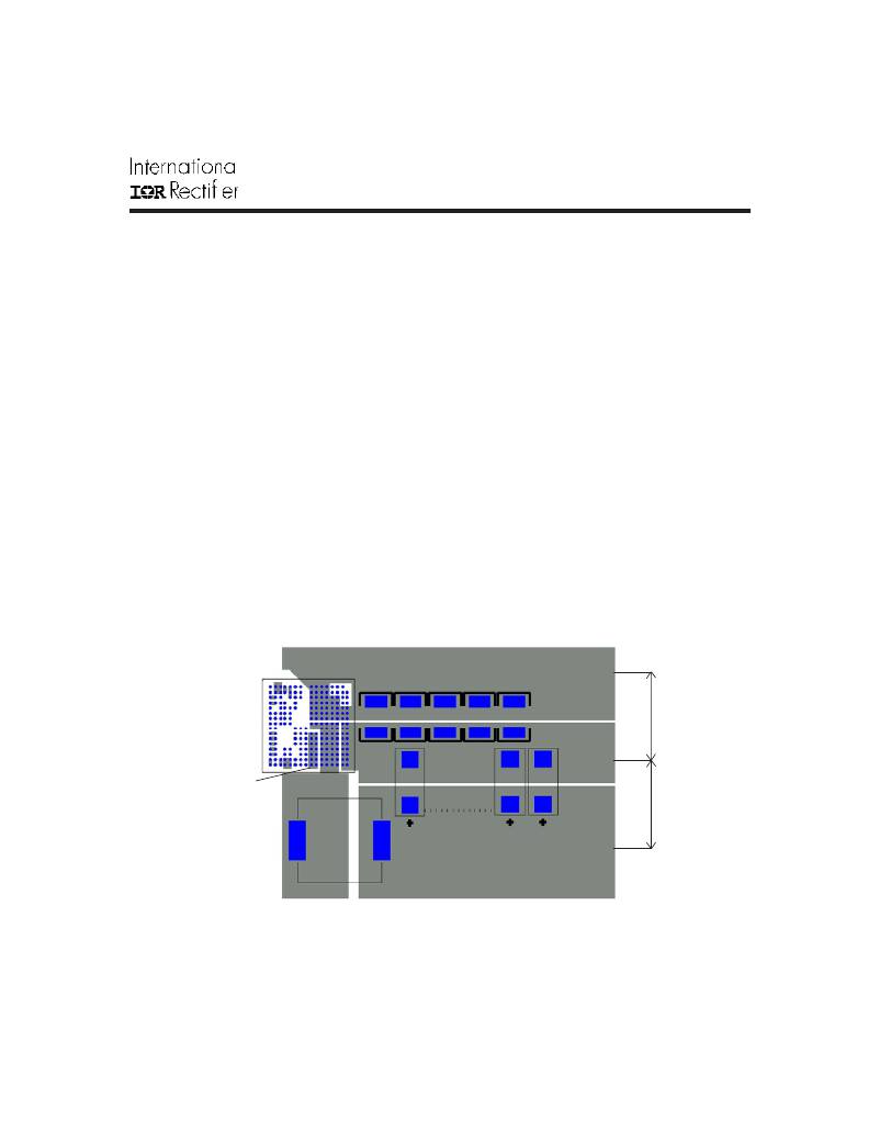
�Layout� Guidelines�
�For� stable� and� noise� free� operation� of� the� whole�
�power� system� it� is� recommended� that� the� designer�
�uses� to� the� following� guidelines.�
�1.� Follow� the� layout� scheme� presented� in� Fig.9.�
�Make� sure� that� the� output� inductor� L1� is� placed� as�
�close� to� the� iP1001� as� possible� to� prevent� noise�
�propagation� that� can� be� caused� by� switching� of�
�power� at� the� switching� node� V� SW� ,� to� sensitive� circuits.�
�2.� Provide� a� mid-layer� solid� ground� with� connections�
�to� the� top� layer� through� vias.� The� two� PGND� pads� of�
�the� iP1001� also� need� to� be� connected� to� the� same�
�ground� plane� through� vias.�
�3.� Do� not� connect� SGND� pins� of� the� iP1001� to� PGND.�
�4.� To� increase� power� supply� noise� immunity,� place�
�input� and� output� capacitors� close� to� one� another,� as�
�shown� in� the� layout� diagram.� This� will� provide� short�
�high� current� paths� that� are� essential� at� the� ground�
�terminals.�
�5.� Although� there� is� a� certain� degree� of� V� IN�
�bypassing� inside� the� iP1001,� the� external� input�
�decoupling� capacitors� should� be� as� close� to� the�
�device� as� possible.�
�6.� In� situations� where� the� load� is� located� at� an�
�appreciable� distance� from� the� iP1001� block,� it� is�
�recommended� that� at� least� one� or� two� capacitors�
�be� placed� close� to� the� iP1001� to� derive� the� V� F�
�signal.�
�7.� The� V� F� connection� to� the� output� capacitors� should�
�be� as� short� as� possible� and� should� be� routed� as�
�far� away� from� noise� generating� traces� as� possible.�
�8.� V� FS� &� GNDS� pins� need� to� be� connected� at� the�
�load� for� remote� sensing.� If� remote� sensing� is� not�
�used� connect� V� FS� to� V� F� and� GNDS� to� PGND.�
�9.� Refer� to� IR� application� note� AN-1029� to� determine�
�what� size� vias� and� what� copper� weight� and�
�thickness� to� use� when� designing� the� PCB.�
�iP1001� Block�
�Input� Caps� (C� IN� )�
�V� IN�
�PGND�
�Input�
�Terminal�
�www.irf.com�
�PGND�
�V� SW�
�Output� Caps� (C� OUT� )�
�Output� Inductor� (L� 1� )�
�Fig� 9.� iP1001� suggested� layout�
�V� OUT�
�Load�
�Terminal�
�13�
�相关PDF资料 |
PDF描述 |
|---|---|
| VI-2NX-EY-F1 | CONVERTER MOD DC/DC 5.2V 50W |
| AGM06DTMN-S189 | CONN EDGECARD 12POS R/A .156 SLD |
| MCP1826S-2502E/DB | IC REG LDO 2.5V 1A SOT223-3 |
| ASM06DTMN-S189 | CONN EDGECARD 12POS R/A .156 SLD |
| MCP1826S-0802E/DB | IC REG LDO 0.8V 1A SOT223-3 |
相关代理商/技术参数 |
参数描述 |
|---|---|
| IP1001-DS-R01 | 制造商:未知厂家 制造商全称:未知厂家 功能描述:Integrated 10/100/1000 Gigabit Ethernet Transceiver |
| IP1001-DS-R02 | 制造商:未知厂家 制造商全称:未知厂家 功能描述:Integrated 10/100/1000 Gigabit Ethernet Transceiver |
| IP1001-DS-R03 | 制造商:未知厂家 制造商全称:未知厂家 功能描述:Integrated 10/100/1000 Gigabit Ethernet Transceiver |
| IP1001-DS-R04 | 制造商:未知厂家 制造商全称:未知厂家 功能描述:Integrated 10/100/1000 Gigabit Ethernet Transceiver |
| IP1001-DS-R05 | 制造商:未知厂家 制造商全称:未知厂家 功能描述:Integrated 10/100/1000 Gigabit Ethernet Transceiver |
发布紧急采购,3分钟左右您将得到回复。