- 您现在的位置:买卖IC网 > PDF目录1807 > IP1201TRPBF (International Rectifier)IC REG BUCK SYNC ADJ 30A 198BGA PDF资料下载
参数资料
| 型号: | IP1201TRPBF |
| 厂商: | International Rectifier |
| 文件页数: | 25/29页 |
| 文件大小: | 0K |
| 描述: | IC REG BUCK SYNC ADJ 30A 198BGA |
| 产品变化通告: | (EP) Parts Discontinuation 25/May/2012 |
| 标准包装: | 750 |
| 系列: | iPOWIR™ |
| 类型: | 降压(降压) |
| 输出类型: | 可调式 |
| 输出数: | 2 |
| 输出电压: | 0.8 V ~ 3.3 V |
| 输入电压: | 3.14 V ~ 5.5 V |
| PWM 型: | 电流模式 |
| 频率 - 开关: | 200kHz ~ 400kHz |
| 电流 - 输出: | 30A |
| 同步整流器: | 是 |
| 工作温度: | -40°C ~ 125°C |
| 安装类型: | 表面贴装 |
| 封装/外壳: | 198-BGA(159 凸块) |
| 包装: | 带卷 (TR) |
| 供应商设备封装: | BGA(15.5x9.25) |
| 配用: | IRDCIP1201-A-ND - BUCK CONV REF DESIGN KIT IP1201 |
第1页第2页第3页第4页第5页第6页第7页第8页第9页第10页第11页第12页第13页第14页第15页第16页第17页第18页第19页第20页第21页第22页第23页第24页当前第25页第26页第27页第28页第29页
�� �
�
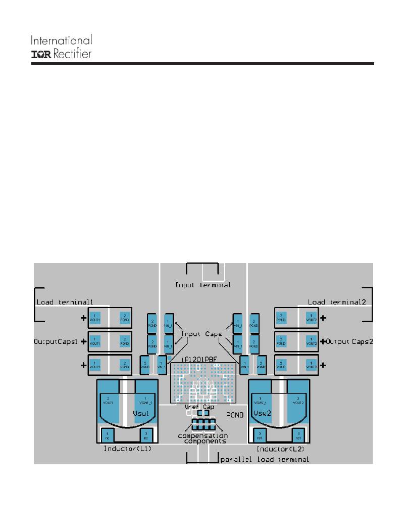
�iP1201PbF�
�Layout� Guidelines�
�For� stable� and� noise� free� operation� of� the� whole�
�power� system,� it� is� recommended� that� the� de-�
�signer� uses� the� following� guidelines:�
�1.� Follow� the� layout� scheme� presented� in� Fig.� 33.�
�Make� sure� that� the� output� inductors� L1� and� L2� are�
�placed� as� close� to� iP1201PbF� as� possible� to� prevent�
�noise� propagation� that� can� be� caused� by� switch-�
�ing� of� power� at� the� switching� node� Vsw,� to� sensi-�
�tive� circuits.�
�2.� Provide� a� mid-layer� solid� ground� plane� with� con-�
�nections� to� the� top� layer� through� vias.� The� PGND�
�pads� of� iP1201PbF� also� need� to� be� connected� to� the�
�same� ground� plane� through� vias.�
�3.� To� increase� power� supply� noise� immunity,� place�
�input� and� output� capacitors� close� to� one� another,�
�as� shown� in� the� layout� diagram.� This� will� provide�
�short� high� current� paths� that� are� essential� at� the�
�ground� terminals.�
�4.� Although� there� is� a� certain� degree� of� V� IN� bypass-�
�ing� inside� the� iP1201PbF,� the� external� input� decoupling�
�capacitors� should� be� as� close� to� the� device� as� pos-�
�sible.�
�5.� The� Feedback� tracks� from� the� outputs� V� OUT1� and�
�V� OUT2� to� FB1� and� FB2� respectively,� should� be� routed�
�as� far� away� from� noise� generating� traces� as� pos-�
�sible.�
�6.� The� compensation� components� and� the� Vref� by-�
�pass� capacitor� should� be� placed� as� close� as� pos-�
�sible� to� their� corresponding� iP1201PbF� pins.�
�7.� For� single� output� configuration,� the� parasitic� paths�
�leading� to� the� common� output� connector� from� each�
�parallel� branch� should� be� symmetrically� routed� to�
�ensure� equal� current� sharing.�
�8.� Refer� to� IR� application� note� AN-1029� to� deter-�
�mine� what� size� vias� and� copper� weight� and� thick-�
�ness� to� use� when� designing� the� PCB.�
�Fig.� 33:� iP1201PbF� suggested� layout�
�www.irf.com�
�25�
�相关PDF资料 |
PDF描述 |
|---|---|
| IP1201TR | IC REG BUCK SYNC ADJ 30A 198BGA |
| IP1202TRPBF | IC REG BUCK SYNC ADJ 30A 198BGA |
| IP1202TR | IC REG BUCK SYNC ADJ 30A 198BGA |
| IP1203TRPBF | IC REG BUCK SYNC ADJ 15A 24LGA |
| IP1203TR | IC REG BUCK SYNC ADJ 15A 24LGA |
相关代理商/技术参数 |
参数描述 |
|---|---|
| IP1202 | 功能描述:开关变换器、稳压器与控制器 DUAL OUTPUT 2-Phase 5.5V to 13.2V 15A RoHS:否 制造商:Texas Instruments 输出电压:1.2 V to 10 V 输出电流:300 mA 输出功率: 输入电压:3 V to 17 V 开关频率:1 MHz 工作温度范围: 安装风格:SMD/SMT 封装 / 箱体:WSON-8 封装:Reel |
| IP1202PBF | 功能描述:开关变换器、稳压器与控制器 DUAL OUTPUT 2-Phase 5.5V to 13.2V 15A RoHS:否 制造商:Texas Instruments 输出电压:1.2 V to 10 V 输出电流:300 mA 输出功率: 输入电压:3 V to 17 V 开关频率:1 MHz 工作温度范围: 安装风格:SMD/SMT 封装 / 箱体:WSON-8 封装:Reel |
| IP1202PBF-EL | 制造商:International Rectifier 功能描述: |
| IP1202TR | 功能描述:开关变换器、稳压器与控制器 DUAL OUTPUT 2-Phase 5.5V to 13.2V 15A RoHS:否 制造商:Texas Instruments 输出电压:1.2 V to 10 V 输出电流:300 mA 输出功率: 输入电压:3 V to 17 V 开关频率:1 MHz 工作温度范围: 安装风格:SMD/SMT 封装 / 箱体:WSON-8 封装:Reel |
| IP1202TRPBF | 功能描述:开关变换器、稳压器与控制器 DUAL OUTPUT 2-Phase 5.5V to 13.2V 15A RoHS:否 制造商:Texas Instruments 输出电压:1.2 V to 10 V 输出电流:300 mA 输出功率: 输入电压:3 V to 17 V 开关频率:1 MHz 工作温度范围: 安装风格:SMD/SMT 封装 / 箱体:WSON-8 封装:Reel |
发布紧急采购,3分钟左右您将得到回复。