- 您现在的位置:买卖IC网 > PDF目录378634 > IP1527A (SEMELAB LTD) CAP .15UF 250V PEN FILM 2825 10% PDF资料下载
参数资料
| 型号: | IP1527A |
| 厂商: | SEMELAB LTD |
| 元件分类: | 稳压器 |
| 英文描述: | CAP .15UF 250V PEN FILM 2825 10% |
| 中文描述: | 0.1 A SWITCHING REGULATOR, PDIP16 |
| 封装: | DIP-16 |
| 文件页数: | 4/6页 |
| 文件大小: | 63K |
| 代理商: | IP1527A |
V
CM
= 1.5 to 5.2V
V
IN
= 8 to 35V
PWM COMPARATOR
V
PIN1
– V
PIN2
≥
150mV
V
PIN2
– V
PIN1
≥
150mV
Zero Duty Cycle
Max. Duty Cycle
V
SHUTDOWN
= 0V
V
SHUTDOWN
= 2V
To Outputs
V
SHUTDOWN
= 2.5V
V
SHUTDOWN
= 2.5V
OUTPUT DRIVERS (each output)
4
T
J
= 25°C
I
SINK
= 20mA
I
SINK
= 100mA
I
SOURCE
= 20mA
I
SOURCE
= 100mA
V
COMP
= High
V
C
= 35V
C
L
= 1nF
C
L
= 1nF
TOTAL STANDBY CURRENT
T
J
= 25°C
T
J
= 25°C
V
IN
= 35V
Output Low Level
Output High Level
Common Mode Rejection
Supply Voltage Rejection
Minimum Duty Cycle
Maximum Duty Cycle
Input Threshold
Input Threshold
Input Bias Current
Soft Start Current
Soft Start Low Level
Shutdown Threshold
Shutdown Input Current
Shutdown Delay
Output Low Level
Output High Level
Undervoltage Lockout
Output Leakage
Rise Time
Fall Time
Supply Current
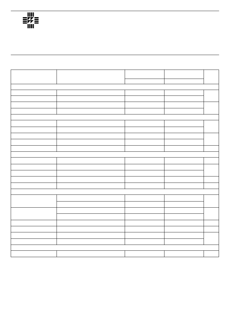
IP1525A
IP1527A
Typ.
IP3525A
IP3527A
Typ.
Parameter
Test Conditions
ERROR AMPLIFIER SECTION (cont.)
3
Min.
Max.
Min.
Max.
Units
0.2
0.5
3.8
5.6
60
75
50
60
0
45
49
0.6
0.9
3.3
3.6
0.05
1.0
25
50
80
0.4
0.6
0.6
1.3
2.0
0.1
1.0
0.2
0.5
0.2
0.4
1.0
2.0
18
19
17
18
5
7
8
200
100
600
50
300
10
20
0.2
0.5
3.8
5.6
60
75
50
60
0
45
49
0.6
0.9
3.3
3.6
0.05
1.0
25
50
80
0.4
0.6
0.6
1.3
2.0
0.1
1.0
0.2
0.5
0.2
0.4
1.0
2.0
18
19
17
18
5
7
8
200
100
600
50
300
10
20
V
dB
%
V
μ
A
μ
A
V
mA
μ
s
V
V
V
μ
A
ns
mA
LAB
SEME
IP1525A SERIES
IP1527A SERIES
Semelab plc.
Telephone (01455) 556565. Telex: 341927. Fax (01455) 552612.
Prelim. 3/95
NOTES
1. Test Conditions unless otherwise stated:
V
IN
= 20V
T
J
= –55 to +125°C for IP1525A / IP1527A
T
J
= 0 to +70°C
for IP3525A / IP3527A
2. Oscillator Section Test Conditions:
f
OSC
= 40kHz
(R
T
= 3.6k
, C
T
= 0.01
μ
F , R
D
= 0)
3. Error Amplifier Section Test Condition:
V
CM
= 5.1V
4. Output Driver Section Test Condition:
V
C
= 20V
ELECTRICAL CHARACTERISTICS
(T
J
= Over Operating Temperature Range unless otherwise stated)
SHUTDOWN SECTION
相关PDF资料 |
PDF描述 |
|---|---|
| IP3526 | REGULATING PULSE WIDTH MODULATOR |
| IP3526D | Regulating Pulse Width Modulator |
| IP3526DW | Regulating Pulse Width Modulator |
| IP3526J | Regulating Pulse Width Modulator |
| IP4011 | 5-CH MOTOR DRIVE IC |
相关代理商/技术参数 |
参数描述 |
|---|---|
| IP1527AJ | 制造商:未知厂家 制造商全称:未知厂家 功能描述:Analog IC |
| IP1527J | 制造商:未知厂家 制造商全称:未知厂家 功能描述:Analog IC |
| IP1531 | 制造商:INTERPION 制造商全称:INTERPION 功能描述:TRIPLE OUTPUT VOLTAGE LDO REGULATOR |
| IP1532 | 制造商:INTERPION 制造商全称:INTERPION 功能描述:TRIPLE OUTPUT VOLTAGE SERIES REGULATOR |
| IP1543 | 制造商:SEME-LAB 制造商全称:Seme LAB 功能描述:POWER SUPPLY SUPERVISORY CIRCUIT |
发布紧急采购,3分钟左右您将得到回复。