- 您现在的位置:买卖IC网 > PDF目录378634 > IP3526 (SEMELAB LTD) REGULATING PULSE WIDTH MODULATOR PDF资料下载
参数资料
| 型号: | IP3526 |
| 厂商: | SEMELAB LTD |
| 元件分类: | 稳压器 |
| 英文描述: | REGULATING PULSE WIDTH MODULATOR |
| 中文描述: | 0.1 A SWITCHING REGULATOR, PDSO18 |
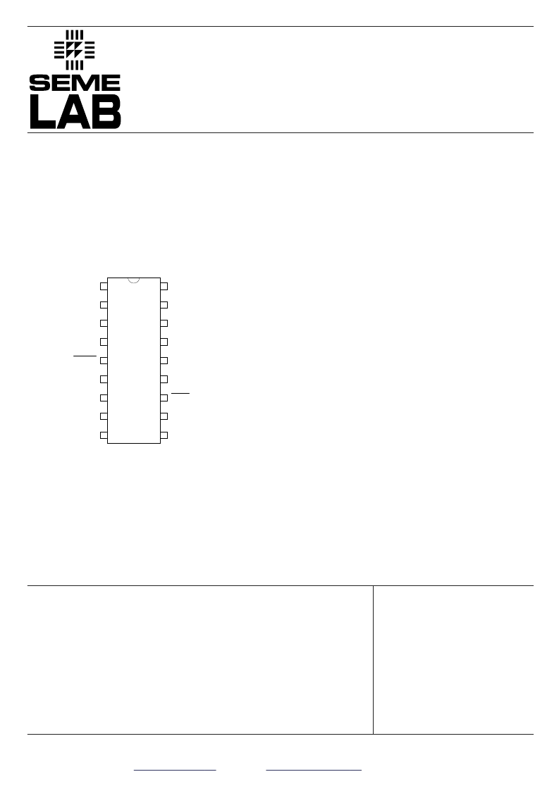
| 封装: | SOIC-18 |
| 文件页数: | 2/6页 |
| 文件大小: | 59K |
| 代理商: | IP3526 |
IP1526 SERIES
4/99
Semelab plc.
E-mail:
sales@semelab.co.uk
Website:
http://www.semelab.co.uk
Telephone +44(0)1455 556565. Fax +44(0)1455 552612.
8
1
2
3
4
5
6
7
14
13
12
11
10
9
15
16
17
18
V
REF
OUTPUT B
GROUND
OUTPUT A
+ERROR
–ERROR
COMPENSATION
SOFTSTART
C
RESET
+CURRENT SENSE
–CURRENT SENSE
SHUTDOWN
C
TIMING
R
TIMING
R
DEADTIME
+V
IN
COLLECTOR
+V
SYNC
+8 to +35V
+4.5 to +35V
0 to 100mA
0 to 20mA
1Hz to 400kHz
2k
to 150k
470pF to 20
μ
F
3% to 50%
–55 to +125°C
0 to +70°C
RECOMMENDED OPERATING CONDITIONS
V
IN
Input Voltage
Collector Voltage
Sink/Source Load Current (Each Output)
Reference Load Current
Oscillator Frequency Range
R
T
Oscillator Timing Resistor
C
T
Oscillator Timing Capacitor
Available Deadtime Range @ 40kHz
Operating Ambient Temperature Range
IP1526
IP3526
DESCRIPTION
The IP1526 and IP3526 high performance monolithic pulse width modulator circuits are designed for fixed-frequency switching
regulators and other power control applications. Included in an 1 8-pin dual-in-line package are a temperature compensated voltage
reference, sawtooth oscillator, error amplifier, pulse width modulator, pulse metering and steering logic, and two low impedance power
drivers. Also included are protective features such as soft-start and under-voltage lockout, digital current limiting, double pulse inhibit, a
data latch for single pulse metering, adjustable deadtime, and provision for symmetry correction inputs. For ease of interface, all digital
control ports are TTL and B-series CMOS compatible. Active LOW logic design allows wired-OR connections for maximum flexibility.
This versatile device can be used to implement single-ended or push-pull switching regulators of either polarity, both transformerless
and transformer coupled.
BLOCK DIAGRAM
相关PDF资料 |
PDF描述 |
|---|---|
| IP3526D | Regulating Pulse Width Modulator |
| IP3526DW | Regulating Pulse Width Modulator |
| IP3526J | Regulating Pulse Width Modulator |
| IP4011 | 5-CH MOTOR DRIVE IC |
| IP4060CX16 | High-speed MultiMediaCard interface filter with ESD protection to IEC61000-4-2 level 4 |
相关代理商/技术参数 |
参数描述 |
|---|---|
| IP3526A | 制造商:SEME-LAB 制造商全称:Seme LAB 功能描述:ADVANCED REGULATING PULSE WIDTH MODULATOR |
| IP3526AD | 制造商:SEME-LAB 制造商全称:Seme LAB 功能描述:Regulating Pulse Width Modulator |
| IP3526ADW | 制造商:SEME-LAB 制造商全称:Seme LAB 功能描述:Regulating Pulse Width Modulator |
| IP3526AJ | 制造商:SEME-LAB 制造商全称:Seme LAB 功能描述:Regulating Pulse Width Modulator |
| IP3526AN | 制造商:未知厂家 制造商全称:未知厂家 功能描述:Analog IC |
发布紧急采购,3分钟左右您将得到回复。