- 您现在的位置:买卖IC网 > PDF目录17410 > IPS2041RTRRPBF (International Rectifier)IC SWITCH IPS 1CH LOW SIDE DPAK PDF资料下载
参数资料
| 型号: | IPS2041RTRRPBF |
| 厂商: | International Rectifier |
| 文件页数: | 2/13页 |
| 文件大小: | 0K |
| 描述: | IC SWITCH IPS 1CH LOW SIDE DPAK |
| 标准包装: | 3,000 |
| 类型: | 低端 |
| 输入类型: | 非反相 |
| 输出数: | 1 |
| 导通状态电阻: | 100 毫欧 |
| 电流 - 输出 / 通道: | 1.4A |
| 电流 - 峰值输出: | 5.5A |
| 电源电压: | 4 V ~ 5.5 V |
| 工作温度: | -40°C ~ 150°C |
| 安装类型: | 表面贴装 |
| 封装/外壳: | TO-252-3,DPak(2 引线+接片),SC-63 |
| 供应商设备封装: | D-Pak |
| 包装: | 带卷 (TR) |
�� �
�
�IPS2041(L)(R)PbF�
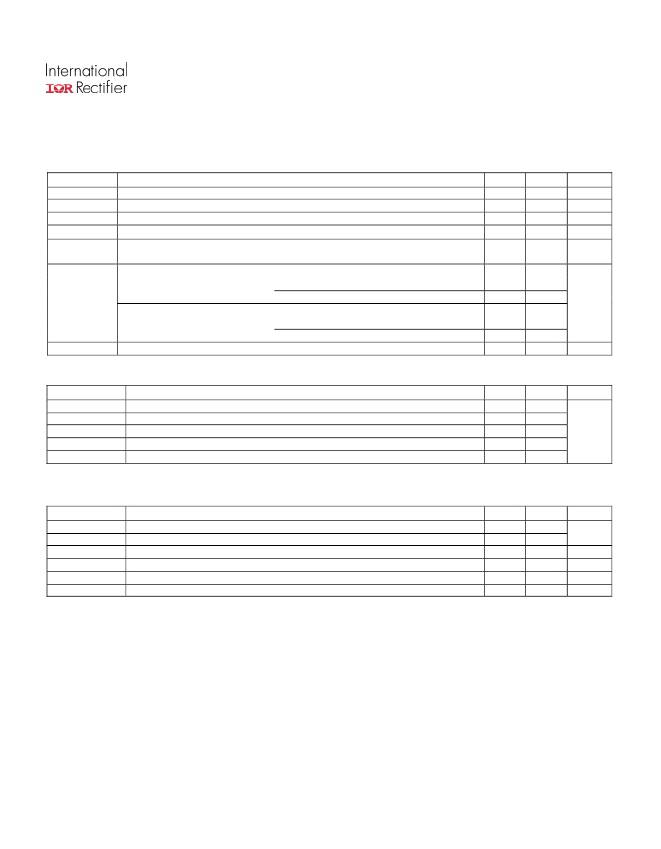
�Absolute� Maximum� Ratings�
�Absolute� maximum� ratings� indicate� sustained� limits� beyond� which� damage� to� the� device� may� occur.� All� voltage� parameters�
�are� referenced� to� Ground� lead.� (Tambient=25°C� unless� otherwise� specified).�
�Symbol�
�Vds�
�Vds� cont.�
�Vin�
�Isd� cont.�
�Pd�
�Parameter�
�Maximum� drain� to� source� voltage�
�Maximum� continuous� drain� to� source� voltage�
�Maximum� input� voltage�
�Max� diode� continuous� current� (limited� by� thermal� dissipation)� Rth=125°C/W�
�Maximum� power� dissipation� (internally� limited� by� thermal� protection)�
�Rth=125C°/W�
�Min.�
�-0.3�
�-�
�-0.3�
�?�
�?�
�Max.�
�60�
�35�
�6�
�1.4�
�1�
�Units�
�V�
�V�
�V�
�A�
�W�
�Electrostatic� discharge� voltage� (Human� body)� C=100pF,� R=1500� ?�
�Between� drain� and� source�
�?�
�4�
�ESD�
�Tj� max.�
�Other� combinations�
�Electrostatic� discharge� voltage� (Machine� Model)� C=200pF,R=0� ?�
�Between� drain� and� source�
�Other� combinations�
�Max.� storage� &� operating� temperature� junction� temperature�
�?�
�?�
�?�
�-40�
�3�
�0.5�
�0.3�
�150�
�kV�
�°C�
�Thermal� Characteristics�
�Symbol�
�Rth1�
�Rth2�
�Rth1�
�Rth2�
�Rth3�
�Parameter�
�Thermal� resistance� junction� to� ambient� IPS2041L�
�Thermal� resistance� junction� to� ambient� with� 1”� square� footprint�
�Thermal� resistance� junction� to� ambient� IPS2041R� D-Pak� std.� footprint�
�Thermal� resistance� junction� to� ambient� IPS2041R� D-Pak� 1”� sqr.� footprint�
�Thermal� resistance� junction� to� case� IPS2041R� D-Pak�
�Typ.�
�100�
�50�
�70�
�50�
�4�
�Max.�
�?�
�?�
�?�
�?�
�?�
�Units�
�°C/W�
�Recommended� Operating� Conditions�
�These� values� are� given� for� a� quick� design.� For� operation� outside� these� conditions,� please� consult� the� application� notes.�
�Symbol�
�VIH�
�VIL�
�Ids�
�Rin�
�Max� L�
�Max.� t� rise�
�Parameter�
�High� level� input� voltage�
�Low� level� input� voltage�
�Continuous� drain� current,� Tambient=85°C,� Tj=125°C,� Vin=5V,Rth=100°C/W�
�Recommended� resistor� in� series� with� IN� pin� to� generate� a� diagnostic�
�Max� recommended� load� inductance� (including� line� inductance)� (1)�
�Max.� input� rising� time�
�Min.�
�4�
�0�
�?�
�0.5�
�?�
�?�
�Max.�
�5.5�
�0.5�
�1.4�
�5�
�10�
�1�
�Units�
�A�
�k� ?�
�mH�
�μs�
�(1)� Higher� inductance� is� possible� if� maximum� load� current� is� limited� -� see� figure� 11�
�www.irf.com�
�2�
�相关PDF资料 |
PDF描述 |
|---|---|
| GCM08DCTH-S288 | CONN EDGECARD 16POS .156 EXTEND |
| EL7154CSZ-T7 | IC PIN DRIVER 10MHZ 3ST 8-SOIC |
| GEM12DRXI | CONN EDGECARD 24POS DIP .156 SLD |
| HCC06DRAH | CONN EDGECARD 12POS R/A .100 SLD |
| GSC05DTEN | CONN EDGECARD 10POS .100 EYELET |
相关代理商/技术参数 |
参数描述 |
|---|---|
| IPS20C-D-G-LF | 制造商:未知厂家 制造商全称:未知厂家 功能描述:Precision Feedback Controllers Fixed and PTAT references |
| IPS20C-SO-G-LF | 制造商:未知厂家 制造商全称:未知厂家 功能描述:Precision Feedback Controllers Fixed and PTAT references |
| IPS20C-SO-G-LF-TR | 制造商:未知厂家 制造商全称:未知厂家 功能描述:Precision Feedback Controllers Fixed and PTAT references |
| IPS20I-D-G-LF | 制造商:未知厂家 制造商全称:未知厂家 功能描述:Precision Feedback Controllers Fixed and PTAT references |
| IPS20N03L G | 功能描述:MOSFET N-CH 30V 30A IPAK RoHS:是 类别:分离式半导体产品 >> FET - 单 系列:- 标准包装:1,000 系列:MESH OVERLAY™ FET 型:MOSFET N 通道,金属氧化物 FET 特点:逻辑电平门 漏极至源极电压(Vdss):200V 电流 - 连续漏极(Id) @ 25° C:18A 开态Rds(最大)@ Id, Vgs @ 25° C:180 毫欧 @ 9A,10V Id 时的 Vgs(th)(最大):4V @ 250µA 闸电荷(Qg) @ Vgs:72nC @ 10V 输入电容 (Ciss) @ Vds:1560pF @ 25V 功率 - 最大:40W 安装类型:通孔 封装/外壳:TO-220-3 整包 供应商设备封装:TO-220FP 包装:管件 |
发布紧急采购,3分钟左右您将得到回复。