- 您现在的位置:买卖IC网 > Datasheet目录331 > IR2151STR (International Rectifier)IC DRVR HALF BRDG SELF-OSC 8SOIC Datasheet资料下载
参数资料
| 型号: | IR2151STR |
| 厂商: | International Rectifier |
| 文件页数: | 2/6页 |
| 文件大小: | 0K |
| 描述: | IC DRVR HALF BRDG SELF-OSC 8SOIC |
| 标准包装: | 2,500 |
| 配置: | 半桥 |
| 输入类型: | 自振荡 |
| 电流 - 峰: | 125mA |
| 配置数: | 1 |
| 输出数: | 2 |
| 高端电压 - 最大(自引导启动): | 600V |
| 电源电压: | 10 V ~ 20 V |
| 工作温度: | -40°C ~ 125°C |
| 安装类型: | 表面贴装 |
| 封装/外壳: | 8-SOIC(0.154",3.90mm 宽) |
| 供应商设备封装: | 8-SOICN |
| 包装: | 带卷 (TR) |
�� �
�
�IR2151�
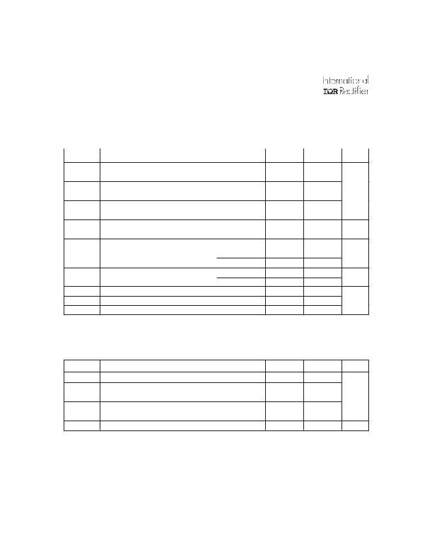
�Absolute� Maximum� Ratings�
�Absolute� maximum� ratings� indicate� sustained� limits� beyond� which� damage� to� the� device� may� occur.� All� voltage� param-�
�eters� are� absolute� voltages� referenced� to� COM.� The� thermal� resistance� and� power� dissipation� ratings� are� measured�
�under� board� mounted� and� still� air� conditions.�
�Symbol�
�V� B�
�V� S�
�V� HO�
�V� LO�
�V� RT�
�V� CT�
�I� CC�
�I� RT�
�dV� s� /dt�
�Definition�
�High� side� floating� supply� voltage�
�High� side� floating� supply� offset� voltage�
�High� side� floating� output� voltage�
�Low� side� output� voltage�
�R� T� voltage�
�C� T� voltage�
�Supply� current� (note� 1)�
�R� T� output� current�
�Allowable� offset� supply� voltage� transient�
�Min.�
�-0.3�
�V� B� -� 25�
�V� S� -� 0.3�
�-0.3�
�-0.3�
�-0.3�
�—�
�-5�
�—�
�Max.�
�625�
�V� B� +� 0.3�
�V� B� +� 0.3�
�V� CC� +� 0.3�
�V� CC� +� 0.3�
�V� CC� +� 0.3�
�25�
�5�
�50�
�Units�
�V�
�mA�
�V/ns�
�P� D�
�Package� power� dissipation� @� T� A� ≤� +25°C�
�(8� lead� DIP)�
�—�
�1.0�
�W�
�(8� lead� SOIC)�
�—�
�0.625�
�R� θ� JA�
�Thermal� resistance,� junction� to� ambient�
�(8� lead� DIP)�
�—�
�125�
�°C/W�
�(8� lead� SOIC)�
�—�
�200�
�T� J�
�Junction� temperature�
�—�
�150�
�T� S�
�T� L�
�Storage� temperature�
�Lead� temperature� (soldering,� 10� seconds)�
�-55�
�—�
�150�
�300�
�°C�
�Recommended� Operating� Conditions�
�The� input/output� logic� timing� diagram� is� shown� in� figure� 1.� For� proper� operation� the� device� should� be� used� within� the�
�recommended� conditions.� The� V� S� offset� rating� is� tested� with� all� supplies� biased� at� 15V� differential.�
�Symbol�
�V� B�
�V� S�
�V� HO�
�V� LO�
�I� CC�
�T� A�
�Definition�
�High� side� sloating� supply� absolute� voltage�
�High� side� floating� supply� offset� voltage�
�High� side� floating� output� voltage�
�Low� side� output� voltage�
�Supply� current� (note� 1)�
�Ambient� temperature�
�Min.�
�V� S� +� 10�
�—�
�V� S�
�0�
�—�
�-40�
�Max.�
�V� S� +� 20�
�600�
�V� B�
�V� CC�
�5�
�125�
�Units�
�V�
�mA�
�°C�
�Note� 1:�
�Because� of� the� IR2151’s� application� specificity� toward� off-line� supply� systems,� this� IC� contains� a� zener� clamp�
�structure� between� the� chip� V� CC� and� COM� which� has� a� nominal� breakdown� voltage� of� 15.6V.� Therefore,� the� IC�
�supply� voltage� is� normally� derived� by� forcing� current� into� the� supply� lead� (typically� by� means� of� a� high� value�
�resistor� connected� between� the� chip� V� CC� and� the� rectified� line� voltage� and� a� local� decoupling� capacitor� from�
�V� CC� to� COM)� and� allowing� the� internal� zener� clamp� circuit� to� determine� the� nominal� supply� voltage.� There-�
�fore,� this� circuit� should� not� be� driven� by� a� DC,� low� impedance� power� source� of� greater� than� V� CLAMP� .�
�2�
�相关PDF资料 |
PDF描述 |
|---|---|
| IR2152 | IC DRVR HALF BRDG SELF-OSC 8-DIP |
| IR21531STRPBF | IC DRIVER HALF BRIDGE OSC 8SOIC |
| IR2153DPBF | IC DVR HALF BRDG SELF-OSC 8-DIP |
| IR2155 | IC DRVR HALF BRDG SELF-OSC 8-DIP |
| IR2181STRPBF | IC DRIVER HIGH/LOW SIDE 8SOIC |
相关代理商/技术参数 |
参数描述 |
|---|---|
| IR2152 | 功能描述:IC DRVR HALF BRDG SELF-OSC 8-DIP RoHS:否 类别:集成电路 (IC) >> PMIC - MOSFET,电桥驱动器 - 外部开关 系列:- 标准包装:50 系列:- 配置:低端 输入类型:非反相 延迟时间:40ns 电流 - 峰:9A 配置数:1 输出数:1 高端电压 - 最大(自引导启动):- 电源电压:4.5 V ~ 35 V 工作温度:-40°C ~ 125°C 安装类型:表面贴装 封装/外壳:TO-263-6,D²Pak(5 引线+接片),TO-263BA 供应商设备封装:TO-263 包装:管件 |
| IR2152S | 制造商:未知厂家 制造商全称:未知厂家 功能描述:Half Bridge Driver. LO Out of Phase with RT. Programmable Oscillating Frequency. 1.2us Deadtime in a 8-lead SOIC package |
| IR2153 | 功能描述:IC DRVR HALF BRDG SELF-OSC 8-DIP RoHS:否 类别:集成电路 (IC) >> PMIC - MOSFET,电桥驱动器 - 外部开关 系列:- 标准包装:50 系列:- 配置:低端 输入类型:非反相 延迟时间:40ns 电流 - 峰:9A 配置数:1 输出数:1 高端电压 - 最大(自引导启动):- 电源电压:4.5 V ~ 35 V 工作温度:-40°C ~ 125°C 安装类型:表面贴装 封装/外壳:TO-263-6,D²Pak(5 引线+接片),TO-263BA 供应商设备封装:TO-263 包装:管件 |
| IR2153_09 | 制造商:IRF 制造商全称:International Rectifier 功能描述:SELF-OSCILLATING HALF-BRIDGE DRIVER |
| IR21531 | 功能描述:IC DRVR HALF BRDG SELF-OSC 8-DIP RoHS:否 类别:集成电路 (IC) >> PMIC - MOSFET,电桥驱动器 - 外部开关 系列:- 标准包装:50 系列:- 配置:低端 输入类型:非反相 延迟时间:40ns 电流 - 峰:9A 配置数:1 输出数:1 高端电压 - 最大(自引导启动):- 电源电压:4.5 V ~ 35 V 工作温度:-40°C ~ 125°C 安装类型:表面贴装 封装/外壳:TO-263-6,D²Pak(5 引线+接片),TO-263BA 供应商设备封装:TO-263 包装:管件 |
发布紧急采购,3分钟左右您将得到回复。