- 您现在的位置:买卖IC网 > PDF目录377498 > IR2181SPbF (International Rectifier) HIGH AND LOW SIDE DRIVER PDF资料下载
参数资料
| 型号: | IR2181SPbF |
| 厂商: | International Rectifier |
| 英文描述: | HIGH AND LOW SIDE DRIVER |
| 中文描述: | 高端和低端驱动 |
| 文件页数: | 2/21页 |
| 文件大小: | 364K |
| 代理商: | IR2181SPBF |
IR2181
(
4
) (S) & (PbF)
2
www.irf.com
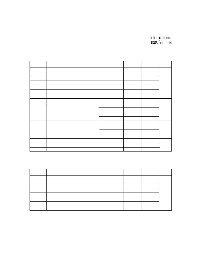
Symbol
Definition
Min.
Max.
Units
V
B
High side floating absolute voltage
-0.3
625
V
S
High side floating supply offset voltage
V
B
- 25
V
B
+ 0.3
V
HO
High side floating output voltage
V
S
- 0.3
V
B
+ 0.3
V
CC
Low side and logic fixed supply voltage
-0.3
25
V
LO
Low side output voltage
-0.3
V
CC
+ 0.3
V
IN
Logic input voltage (HIN & LIN - IR2181/IR21814)
V
SS
- 0.3 V
SS
+ 10
V
SS
Logic ground (IR21814 only)
V
CC
- 25
V
CC
+ 0.3
dV
S
/dt
Allowable offset supply voltage transient
—
50
V/ns
P
D
Package power dissipation @ T
A
≤
+25
°
C
(8-lead PDIP)
—
1.0
(8-lead SOIC)
—
0.625
(14-lead PDIP)
—
1.6
(14-lead SOIC)
—
1.0
Rth
JA
Thermal resistance, junction to ambient
(8-lead PDIP)
—
125
(8-lead SOIC)
—
200
(14-lead PDIP)
—
75
(14-lead SOIC)
—
120
T
J
Junction temperature
—
150
T
S
Storage temperature
-50
150
T
L
Lead temperature (soldering, 10 seconds)
—
300
Absolute Maximum Ratings
Absolute maximum ratings indicate sustained limits beyond which damage to the device may occur. All voltage param-
eters are absolute voltages referenced to COM. The thermal resistance and power dissipation ratings are measured
under board mounted and still air conditions.
V
°
C/W
W
°
C
Note 1: Logic operational for V
S
of -5 to +600V. Logic state held for V
S
of -5V to -V
BS
. (Please refer to the Design Tip
DT97-3 for more details).
Note 2: HIN and LIN pins are internally clamped with a 5.2V zener diode.
VB
High side floating supply absolute voltage
V
S
+ 10
V
S
+ 20
V
S
High side floating supply offset voltage
Note 1
600
V
HO
High side floating output voltage
V
S
V
B
V
CC
Low side and logic fixed supply voltage
10
20
V
LO
Low side output voltage
0
V
CC
V
IN
Logic input voltage (HIN & LIN - IR2181/IR21814) V
SS
V
SS
+ 5
V
SS
Logic ground (IR21814/IR21824 only)
-5
5
T
A
Ambient temperature
-40
125
°
C
V
Symbol
Definition
Min.
Max.
Units
Recommended Operating Conditions
The Input/Output logic timing diagram is shown in figure 1. For proper operation the device should be used within the
recommended conditions. The V
S
and V
SS
offset rating are tested with all supplies biased at 15V differential.
相关PDF资料 |
PDF描述 |
|---|---|
| IR21814SPBF | HIGH AND LOW SIDE DRIVER |
| IR2181PBF | HIGH AND LOW SIDE DRIVER |
| IR2183S | HALF-BRIDGE DRIVER |
| IR2183 | HALF-BRIDGE DRIVER |
| IR21834 | HALF-BRIDGE DRIVER |
相关代理商/技术参数 |
参数描述 |
|---|---|
| IR2181SPBF-EL | 制造商:International Rectifier 功能描述: |
| IR2181STRPBF | 功能描述:功率驱动器IC Hi&Lw Sd Drvr Soft Trn On Non Invrt RoHS:否 制造商:Micrel 产品:MOSFET Gate Drivers 类型:Low Cost High or Low Side MOSFET Driver 上升时间: 下降时间: 电源电压-最大:30 V 电源电压-最小:2.75 V 电源电流: 最大功率耗散: 最大工作温度:+ 85 C 安装风格:SMD/SMT 封装 / 箱体:SOIC-8 封装:Tube |
| IR2183 | 功能描述:IC DRIVER HALF BRIDGE 600V 8-DIP RoHS:否 类别:集成电路 (IC) >> PMIC - MOSFET,电桥驱动器 - 外部开关 系列:- 标准包装:50 系列:- 配置:高端 输入类型:非反相 延迟时间:200ns 电流 - 峰:250mA 配置数:1 输出数:1 高端电压 - 最大(自引导启动):600V 电源电压:12 V ~ 20 V 工作温度:-40°C ~ 125°C 安装类型:通孔 封装/外壳:8-DIP(0.300",7.62mm) 供应商设备封装:8-DIP 包装:管件 其它名称:*IR2127 |
| IR21834 | 功能描述:IC DRIVER HALF-BRIDGE 14-DIP RoHS:否 类别:集成电路 (IC) >> PMIC - MOSFET,电桥驱动器 - 外部开关 系列:- 标准包装:50 系列:- 配置:高端 输入类型:非反相 延迟时间:200ns 电流 - 峰:250mA 配置数:1 输出数:1 高端电压 - 最大(自引导启动):600V 电源电压:12 V ~ 20 V 工作温度:-40°C ~ 125°C 安装类型:通孔 封装/外壳:8-DIP(0.300",7.62mm) 供应商设备封装:8-DIP 包装:管件 其它名称:*IR2127 |
| IR21834PBF | 功能描述:功率驱动器IC Hlf Brdg Drvr Sft Trn On Lw Sd Invrt RoHS:否 制造商:Micrel 产品:MOSFET Gate Drivers 类型:Low Cost High or Low Side MOSFET Driver 上升时间: 下降时间: 电源电压-最大:30 V 电源电压-最小:2.75 V 电源电流: 最大功率耗散: 最大工作温度:+ 85 C 安装风格:SMD/SMT 封装 / 箱体:SOIC-8 封装:Tube |
发布紧急采购,3分钟左右您将得到回复。