- 您现在的位置:买卖IC网 > PDF目录1810 > IR3841MTRPBF (International Rectifier)IC REG BUCK SYNC ADJ 8A 15QFN PDF资料下载
参数资料
| 型号: | IR3841MTRPBF |
| 厂商: | International Rectifier |
| 文件页数: | 27/32页 |
| 文件大小: | 0K |
| 描述: | IC REG BUCK SYNC ADJ 8A 15QFN |
| 产品培训模块: | SupIRBuck? Family and POL Design Tools Overview |
| 标准包装: | 4,000 |
| 系列: | SupIRBuck™ |
| 类型: | 降压(降压) |
| 输出类型: | 可调式 |
| 输出数: | 1 |
| 输出电压: | 0.7 V ~ 14.4 V |
| 输入电压: | 1.5 V ~ 16 V |
| PWM 型: | 电压模式 |
| 频率 - 开关: | 225kHz ~ 1.65MHz |
| 电流 - 输出: | 8A |
| 同步整流器: | 是 |
| 工作温度: | -40°C ~ 125°C |
| 安装类型: | 表面贴装 |
| 封装/外壳: | 15-PowerVQFN |
| 包装: | 带卷 (TR) |
| 供应商设备封装: | PQFN(5x6) |
第1页第2页第3页第4页第5页第6页第7页第8页第9页第10页第11页第12页第13页第14页第15页第16页第17页第18页第19页第20页第21页第22页第23页第24页第25页第26页当前第27页第28页第29页第30页第31页第32页
�� �
�
�IR3841MPbF�
�Layout� Considerations�
�Vin�
�PGnd�
�PGnd�
�capacitor� at� the� Sw� pin.�
�AGnd� Vout�
�The� layout� is� very� important� when� designing� high�
�frequency� switching� converters.� Layout� will� affect�
�noise� pickup� and� can� cause� a� good� design� to�
�perform� with� less� than� expected� results.�
�Make� all� the� connections� for� the� power�
�components� in� the� top� layer� with� wide,� copper�
�filled� areas� or� polygons.� In� general,� it� is� desirable�
�to� make� proper� use� of� power� planes� and�
�polygons� for� power� distribution� and� heat�
�dissipation.�
�The� inductor,� output� capacitors� and� the� IR3841�
�should� be� as� close� to� each� other� as� possible.�
�This� helps� to� reduce� the� EMI� radiated� by� the�
�power� traces� due� to� the� high� switching� currents�
�through� them.� Place� the� input� capacitor� directly� at�
�the� Vin� pin� of� IR3841.�
�The� feedback� part� of� the� system� should� be� kept�
�away� from� the� inductor� and� other� noise� sources.�
�The� critical� bypass� components� such� as�
�capacitors� for� Vcc� should� be� close� to� their�
�respective� pins.� It� is� important� to� place� the�
�feedback� components� including� feedback�
�resistors� and� compensation� components� close� to�
�The� connection� between� the� OCSet� resistor� and�
�the� Sw� pin� should� not� share� any� trace� with� the�
�connection� between� the� bootstrap� capacitor� and�
�the� Sw� pin.� Instead,� it� is� recommended� to� use� a�
�Kelvin� connection� of� the� trace� from� the� OCSet�
�resistor� and� the� trace� from� the� bootstrap�
�Vin�
�VoutAGnd�
�In� a� multilayer� PCB� use� one� layer� as� a� power�
�ground� plane� and� have� a� control� circuit� ground�
�(analog� ground),� to� which� all� signals� are�
�referenced.� The� goal� is� to� localize� the� high�
�current� path� to� a� separate� loop� that� does� not�
�interfere� with� the� more� sensitive� analog� control�
�function.� These� two� grounds� must� be� connected�
�together� on� the� PC� board� layout� at� a� single� point.�
�The� Power� QFN� is� a� thermally� enhanced�
�package.� Based� on� thermal� performance� it� is�
�recommended� to� use� at� least� a� 4-layers� PCB.� To�
�effectively� remove� heat� from� the� device� the�
�exposed� pad� should� be� connected� to� the� ground�
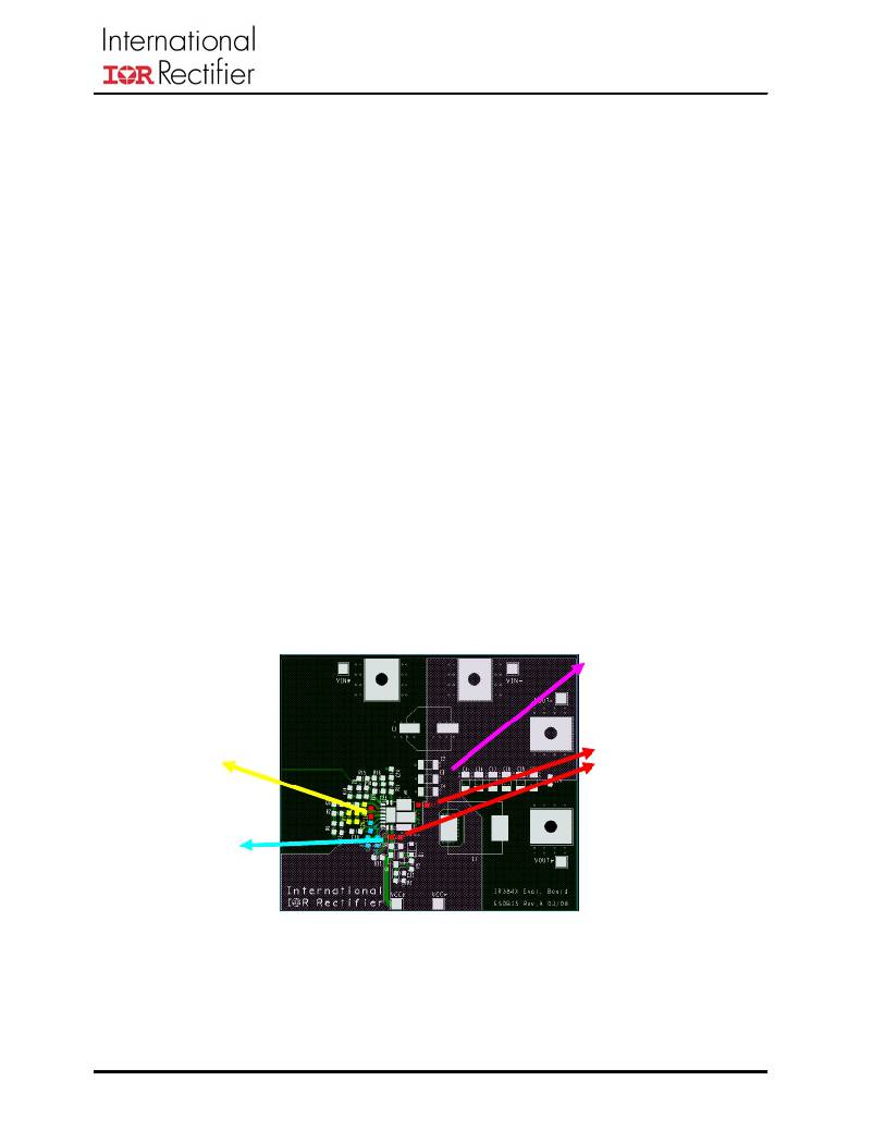
�plane� using� vias.� Figure� 25� illustrates� the�
�implementation� of� the� layout� guidelines� outlined�
�above,� on� the� IRDC3841� 4� layer� demoboard.�
�Fb� and� Comp� pins.�
�Enough� copper� &�
�minimum� length�
�ground� path� between�
�Input� and� Output�
�PGnd�
�Compensation� parts�
�should� be� placed� as� close�
�as� possible� to�
�the� Comp� pin� .�
�Vin�
�Vin�
�PGnd�
�All� bypass� caps�
�should� be� placed� as�
�close� as� possible� to�
�their� connecting�
�pins.�
�AGnd�
�Resistors� Rt� and�
�Rocset� should� be�
�placed� as� close� as�
�possible� to� their� pins.�
�AGnd�
�Vout� Vout�
�Fig.25a.� IRDC3841� demoboard� layout�
�considerations� –� Top� Layer�
�06/18/09�
�27�
�相关PDF资料 |
PDF描述 |
|---|---|
| IR3841WMTRPBF | IC REG BUCK SYNC ADJ 8A 15QFN |
| IR3842AMTRPBF | IC REG BUCK SYNC ADJ 6A QFN |
| IR3842MTRPBF | IC REG BUCK SYNC ADJ 4A 15QFN |
| IR3842WMTRPBF | IC REG BUCK SYNC ADJ 4A 15QFN |
| IR3843AMTRPBF | IC REG BUCK SYNC ADJ 3A QFN |
相关代理商/技术参数 |
参数描述 |
|---|---|
| IR3841WMPBF | 制造商:IRF 制造商全称:International Rectifier 功能描述:HIGHLY EFFICIENT INTEGRATED 8A SYNCHRONOUS BUCK REGULATOR |
| IR3841WMPBF_12 | 制造商:IRF 制造商全称:International Rectifier 功能描述:HIGHLY EFFICIENT INTEGRATED 8A SYNCHRONOUS BUCK REGULATOR |
| IR3841WMTR1PBF | 功能描述:直流/直流开关调节器 8A SupIRBuck Reg 250-1500kHz, 1.5-16V RoHS:否 制造商:International Rectifier 最大输入电压:21 V 开关频率:1.5 MHz 输出电压:0.5 V to 0.86 V 输出电流:4 A 输出端数量: 最大工作温度: 安装风格:SMD/SMT 封装 / 箱体:PQFN 4 x 5 |
| IR3841WMTRPBF | 功能描述:直流/直流开关调节器 8A SupIRBuck Reg 250-1500kHz, 1.5-16V RoHS:否 制造商:International Rectifier 最大输入电压:21 V 开关频率:1.5 MHz 输出电压:0.5 V to 0.86 V 输出电流:4 A 输出端数量: 最大工作温度: 安装风格:SMD/SMT 封装 / 箱体:PQFN 4 x 5 |
| IR3842AMPBF | 制造商:IRF 制造商全称:International Rectifier 功能描述:HIGHLY EFFICIENT INTEGRATED 6A SYNCHRONOUS BUCK REGULATOR |
发布紧急采购,3分钟左右您将得到回复。