- 您现在的位置:买卖IC网 > PDF目录384503 > IRHM8360 (International Rectifier) REPETITIVE AVALANCHE AND dv/dt RATED PDF资料下载
参数资料
| 型号: | IRHM8360 |
| 厂商: | International Rectifier |
| 英文描述: | REPETITIVE AVALANCHE AND dv/dt RATED |
| 中文描述: | 重复性雪崩和dv / dt受好评 |
| 文件页数: | 2/12页 |
| 文件大小: | 332K |
| 代理商: | IRHM8360 |
IRHM7360, IRHM8360 Devices
2
www.irf.com
nA
μ
A
Thermal Resistance
Parameter
RthJC
Junction-to-Case
RthCS
Case-to-Sink
RthJA
Junction-to-Ambient
Min Typ Max
—
—
—
0.21
—
—
Units
Test Conditions
0.5
—
48
°C/W
Typical socket mount
Pre-Irradiation
Electrical Characteristics
@ Tj = 25°C (Unless Otherwise Specified)
Parameter
Drain-to-Source Breakdown Voltage
BVDSS/
TJ Temperature Coefficient of Breakdown
Voltage
RDS(on)
Static Drain-to-Source On-State
Resistance
VGS(th)
Gate Threshold Voltage
gfs
Forward Transconductance
IDSS
Zero Gate Voltage Drain Current
Min
400
—
Typ
—
0.45
Max Units
—
—
Test Conditions
VGS = 0V, ID = 1.0mA
Reference to 25°C, ID = 1.0mA
BVDSS
V
V/°C
—
—
2.0
6.0
—
—
—
—
—
—
—
—
0.22
0.25
4.0
—
50
250
VGS = 12V, ID = 14A
VGS = 12V, ID = 22A
VDS = VGS, ID = 1.0mA
VDS > 15V, IDS = 14A
VDS= 0.8 x Max Rating,VGS=0V
VDS = 0.8 x Max Rating
VGS = 0V, TJ = 125°C
VGS = 20V
VGS = -20V
VGS = 12V, ID =22A
VDS = Max Rating x 0.5
V
S (
)
IGSS
IGSS
Qg
Qgs
Qgd
td
(on)
tr
td
(off)
tf
LD
Gate-to-Source Leakage Forward
Gate-to-Source Leakage Reverse
Total Gate Charge
Gate-to-Source Charge
Gate-to-Drain (‘Miller’) Charge
Turn-On Delay Time
Rise Time
Turn-Off Delay Time
Fall Time
Internal Drain Inductance
—
—
—
—
—
—
—
—
—
—
—
—
—
—
—
—
—
—
—
8.7
100
-100
210
45
120
33
59
140
75
—
nC
VDD = 200V, ID = 22A,
RG = 2.35
LS
Internal Source Inductance
—
8.7
—
Ciss
Coss
Crss
Input Capacitance
Output Capacitance
Reverse Transfer Capacitance
—
—
—
5600
990
380
—
—
—
VGS = 0V, VDS = 25V
f = 1.0MHz
pF
nH
ns
Measured from drain
lead, 6mm (0.25 in)
from package to center
of die.
Measured from source
lead, 6mm (0.25 in)
from package to
source bonding pad.
Modified MOSFET sym-
inductances.
Source-Drain Diode Ratings and Characteristics
Parameter
IS
Continuous Source Current (Body Diode)
ISM
Pulse Source Current (Body Diode)
Min Typ
—
—
Max Units
22
88
Test Conditions
—
—
VSD
trr
QRR
ton
Diode Forward Voltage
Reverse Recovery Time
Reverse Recovery Charge
—
—
—
—
—
—
1.8
1000
11
V
ns
μ
C
T
j
= 25°C, IS = 22A, VGS = 0V
Tj = 25°C, IF =22A, di/dt
≤
100A/
μ
s
VDD
≤
50V
Forward Turn-On Time
Intrinsic turn-on time is negligible. Turn-on speed is substantially controlled by LS + LD.
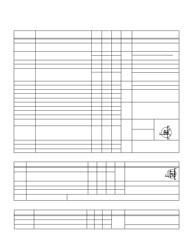
A
Modified MOSFET symbol
showing the integral reverse
p-n junction rectifier.
相关PDF资料 |
PDF描述 |
|---|---|
| IRHM7360SE | TRANSISTOR N-CHANNEL(BVdss=400V, Rds(on)=0.20ohm, Id=22A) |
| IRHM7450 | REPETITIVE AVALANCHE AND dv/dt RATED |
| IRHM7450SE | TRANSISTOR N-CHANNEL(BVdss=500V, Rds(on)=0.51ohm, Id=12A) |
| IRHM8450 | REPETITIVE AVALANCHE AND dv/dt RATED |
| IRHM9064 | TRANSISTOR P-CHANNEL(BVdss=-60V, Rds(on)=0.060ohm, Id=-35*A) |
相关代理商/技术参数 |
参数描述 |
|---|---|
| IRHM8360D | 制造商:未知厂家 制造商全称:未知厂家 功能描述:TRANSISTOR | MOSFET | N-CHANNEL | 400V V(BR)DSS | 22A I(D) | TO-254VAR |
| IRHM8360U | 制造商:未知厂家 制造商全称:未知厂家 功能描述:TRANSISTOR | MOSFET | N-CHANNEL | 400V V(BR)DSS | 22A I(D) | TO-254VAR |
| IRHM8450 | 制造商:International Rectifier 功能描述:HEXFET, HIREL, RAD HARD,G4 - Bulk |
| IRHM8450D | 制造商:未知厂家 制造商全称:未知厂家 功能描述:TRANSISTOR | MOSFET | N-CHANNEL | 500V V(BR)DSS | 11A I(D) | TO-254AA |
| IRHM8450U | 制造商:未知厂家 制造商全称:未知厂家 功能描述:TRANSISTOR | MOSFET | N-CHANNEL | 500V V(BR)DSS | 11A I(D) | TO-254AA |
发布紧急采购,3分钟左右您将得到回复。