- 您现在的位置:买卖IC网 > PDF目录261501 > IRKT71-10S90PBF 109.9 A, 1000 V, SCR, TO-240AA PDF资料下载
参数资料
| 型号: | IRKT71-10S90PBF |
| 元件分类: | 晶闸管 |
| 英文描述: | 109.9 A, 1000 V, SCR, TO-240AA |
| 文件页数: | 4/10页 |
| 文件大小: | 166K |
| 代理商: | IRKT71-10S90PBF |
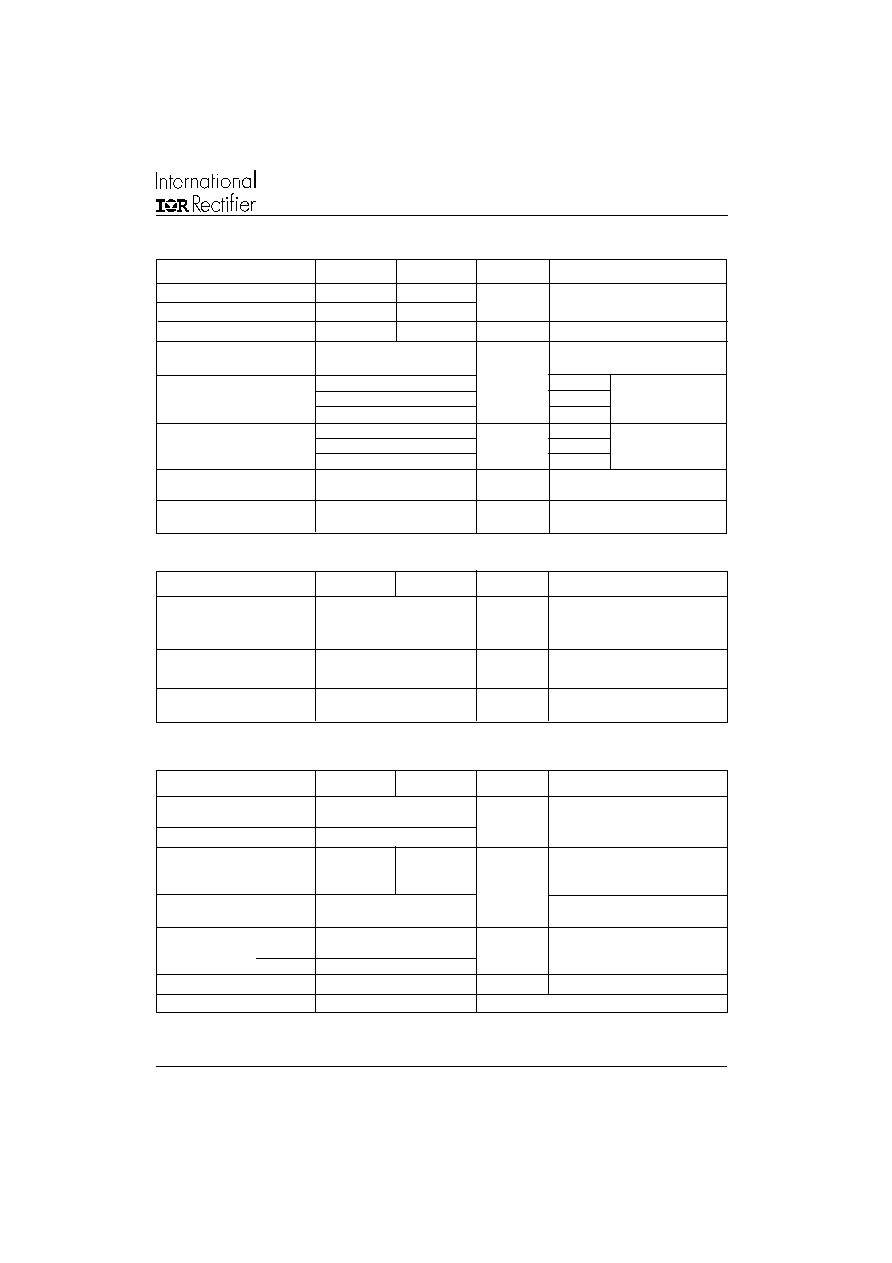
IRK.71, .91 Series
3
Bulletin I27132 rev. D 09/97
www.irf.com
I
RRM
Max. peak reverse and
I
DRM
off-state leakage current
at V
RRM, VDRM
2500
(1 min)
50 Hz, circuit to base, all terminals
3500
(1 sec)
shorted
dv/dt Max. critical rate of rise
T
J
= 125oC, linear to 0.67 V
DRM
,
of off-state voltage (5)
gate open circuit
T
J
Junction operating
temperature range
T
stg
Storage temp. range
- 40 to 125
R
thJC
Max. internal thermal
resistance, junction
0.165
0.135
Per module, DC operation
to case
R
thCS
Typical thermal resistance
case to heatsink
T
Mounting torque ± 10%
to heatsink
busbar
3
wt
Approximate weight
83 (3)
g (oz)
Case style
TO-240AA
JEDEC
15
mA
T
J
= 125 oC, gate open circuit
Thermal and Mechanical Specifications
500
V/
s
Parameters
IRK.71
IRK.91
Units
Conditions
- 40 to 125
0.1
5
Triggering
Blocking
(5) Available with dv/dt = 1000V/
s, to complete code add S90 i.e. IRKT91/16 S90.
A mounting compound is recommended
and the torque should be rechecked after
a period of 3 hours to allow for the
spread of the compound
K/W
Nm
Mounting surface flat, smooth and greased.
Flatness <0.03 mm; roughness
< 0.02mm
V
INS
RMS isolation voltage
V
P
GM
Max. peak gate power
12
P
G(AV) Max. average gate power
3.0
I
GM
Max. peak gate current
3.0
A
-V
GM
Max. peak negative
gate voltage
V
GT
Max. gate voltage
4.0
T
J = - 40°C
required to trigger
2.5
T
J = 25°C
1.7
TJ = 125°C
I
GT
Max. gate current
270
TJ= - 40°C
required to trigger
150
mA
T
J = 25°C
80
T
J = 125°C
V
GD
Max. gate voltage
T
J = 125
oC,
that will not trigger
rated V
DRM
applied
I
GD
Max. gate current
T
J
= 125oC,
that will not trigger
rated V
DRM
applied
Parameters
IRK.71
IRK.91
Units
Conditions
0.25
V
6mA
W
V
10
Anode supply = 6V
resistive load
Anode supply = 6V
resistive load
°C
Parameters
IRK.71
IRK.91
Units
Conditions
相关PDF资料 |
PDF描述 |
|---|---|
| IRKT71-14S90PBF | 109.9 A, 1400 V, SCR, TO-240AA |
| IRKUF180-06FPN | 282.6 A, 600 V, SCR |
| IRKUF180-06FP | 282.6 A, 600 V, SCR |
| IRKUF200-06FPN | 314 A, 600 V, SCR |
| IRKUF180-08FP | 282.6 A, 800 V, SCR |
相关代理商/技术参数 |
参数描述 |
|---|---|
| IRKT7112 | 制造商:IR 功能描述:POWER MODULE |
| IRKT71-12 | 制造商:未知厂家 制造商全称:未知厂家 功能描述:THYRISTOR MODULE|SCR DOUBLER|1.2KV V(RRM)|70A I(T) |
| IRKT71-12A | 制造商:IRF 制造商全称:International Rectifier 功能描述:THYRISTOR/ DIODE and THYRISTOR/ THYRISTOR |
| IRKT7112AS90 | 制造商:IRF 制造商全称:International Rectifier 功能描述:ADD-A-pak GEN V Power Modules THYRISTOR/ DIODE and THYRISTOR/ THYRISTOR |
| IRKT71-12AS90 | 制造商:IRF 制造商全称:International Rectifier 功能描述:THYRISTOR/ DIODE and THYRISTOR/ THYRISTOR |
发布紧急采购,3分钟左右您将得到回复。