- 您现在的位置:买卖IC网 > PDF目录360969 > IRLI3103 PDF资料下载
参数资料
| 型号: | IRLI3103 |
| 文件页数: | 2/8页 |
| 文件大小: | 151K |
| 代理商: | IRLI3103 |
IRLI3103
Parameter
Min. Typ. Max. Units
30
–––
–––
0.037 –––
–––
––– 0.014
–––
––– 0.019
1.0
–––
23
–––
–––
–––
–––
–––
–––
–––
–––
–––
–––
–––
–––
–––
–––
–––
–––
9.0
–––
210
–––
20
–––
54
Conditions
V
GS
= 0V, I
D
= 250μA
Reference to 25°C, I
D
= 1mA
V
GS
= 10V, I
D
= 23A
V
GS
= 4.5V, I
D
= 19A
V
DS
= V
GS
, I
D
= 250μA
V
DS
= 25V, I
D
= 34A
V
DS
= 30V, V
GS
= 0V
V
DS
= 24V, V
GS
= 0V, T
J
= 150°C
V
GS
= 20V
V
GS
= -20V
I
D
= 34A
V
DS
= 24V
V
GS
= 4.5V, See Fig. 6 and 13
V
DD
= 15V
I
D
= 34A
R
G
= 3.4
,
V
GS
= 4.5V
R
D
= 0.43
,
See Fig. 10
Between lead,
6mm (0.25in.)
from package
and center of die contact
V
GS
= 0V
V
DS
= 25V
= 1.0MHz, See Fig. 5
= 1.0MHz
V
(BR)DSS
V
(BR)DSS
/
T
J
Breakdown Voltage Temp. Coefficient
Drain-to-Source Breakdown Voltage
–––
V
V/°C
V
GS(th)
g
fs
Gate Threshold Voltage
Forward Transconductance
2.0
–––
25
250
100
-100
50
14
28
–––
–––
–––
–––
V
S
μA
Gate-to-Source Forward Leakage
Gate-to-Source Reverse Leakage
Total Gate Charge
Gate-to-Source Charge
Gate-to-Drain ("Miller") Charge
Turn-On Delay Time
Rise Time
Turn-Off Delay Time
Fall Time
nA
Q
g
Q
gs
Q
gd
t
d(on)
t
r
t
d(off)
t
f
nC
ns
C
iss
C
oss
C
rss
C
Input Capacitance
Output Capacitance
Reverse Transfer Capacitance
Drain to Sink Capacitance
–––
–––
–––
–––
1600
640
320
12
–––
–––
–––
–––
Electrical Characteristics @ T
J
= 25°C (unless otherwise specified)
R
DS(on)
Static Drain-to-Source On-Resistance
I
GSS
nH
L
S
Internal Source Inductance
–––
7.5
–––
L
D
Internal Drain Inductance
–––
4.5
–––
I
DSS
Drain-to-Source Leakage Current
pF
Notes:
Repetitive rating; pulse width limited by
max. junction temperature. ( See fig. 11 )
V
DD
= 15V, starting T
J
= 25°C, L = 300μH
R
G
= 25
, I
AS
= 34A. (See Figure 12)
t=60s, =60Hz
I
SD
≤
34A, di/dt
≤
140A/μs, V
DD
≤
V
(BR)DSS
,
T
J
≤
175°C
Uses IRL3103 data and test conditions
Pulse width
≤
300μs; duty cycle
≤
2%.
Parameter
Min. Typ. Max. Units
Conditions
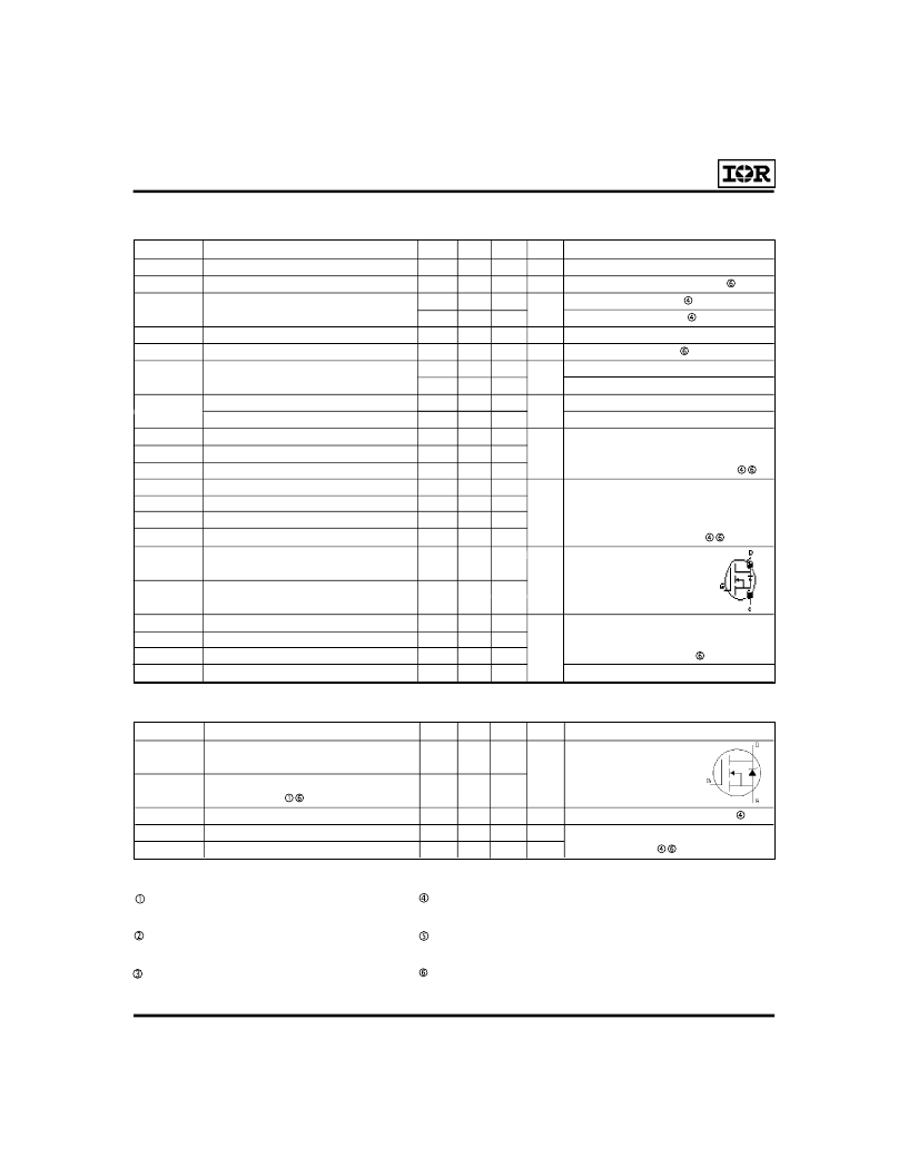
MOSFET symbol
showing the
integral reverse
p-n junction diode.
T
J
= 25°C, I
S
= 23A, V
GS
= 0V
T
J
= 25°C, I
F
= 34A
di/dt = 100A/μs
I
S
Continuous Source Current
(Body Diode)
Pulsed Source Current
(Body Diode)
Diode Forward Voltage
Reverse Recovery Time
Reverse Recovery Charge
–––
–––
I
SM
–––
–––
V
SD
t
rr
Q
rr
–––
–––
–––
–––
81
210
1.3
120
310
V
ns
nC
Source-Drain Ratings and Characteristics
A
220
38
相关PDF资料 |
PDF描述 |
|---|---|
| IRLI3705G | TRANSISTOR | MOSFET | N-CHANNEL | 50V V(BR)DSS | 45A I(D) | TO-220VAR |
| IRLI3103 | HEXFET Power MOSFET(HEXFET 功率MOS场效应管) |
| IRLI520G | TRANSISTOR | MOSFET | N-CHANNEL | 100V V(BR)DSS | 7.2A I(D) | SOT-186 |
| IRLI530G | TRANSISTOR | MOSFET | N-CHANNEL | 100V V(BR)DSS | 9.7A I(D) | SOT-186 |
| IRLI540G | |
相关代理商/技术参数 |
参数描述 |
|---|---|
| IRLI3215PBF | 制造商:International Rectifier 功能描述: |
| IRLI3303 | 制造商:IRF 制造商全称:International Rectifier 功能描述:HEXFET Power MOSFET |
| IRLI3615 | 制造商:IRF 制造商全称:International Rectifier 功能描述:HEXFET Power MOSFET |
| IRLI3615HR | 制造商:International Rectifier 功能描述:Trans MOSFET N-CH 150V 14A 3-Pin(3+Tab) TO-220 |
| IRLI3615PBF | 制造商:International Rectifier 功能描述:MOSFET N 150V 14A TO-220FP |
发布紧急采购,3分钟左右您将得到回复。