- 您现在的位置:买卖IC网 > PDF目录384507 > IRLI520N (International Rectifier) Power MOSFET PDF资料下载
参数资料
| 型号: | IRLI520N |
| 厂商: | International Rectifier |
| 英文描述: | Power MOSFET |
| 中文描述: | 功率MOSFET |
| 文件页数: | 2/2页 |
| 文件大小: | 37K |
| 代理商: | IRLI520N |
IRLI520N
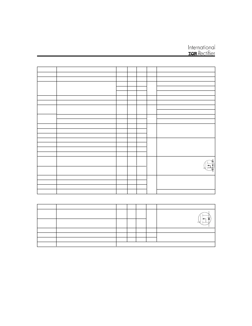
Parameter
Min. Typ. Max. Units
100
–––
–––
0.11
–––
–––
–––
–––
–––
–––
1.0
–––
3.1
–––
–––
–––
–––
–––
–––
–––
–––
–––
–––
–––
–––
–––
–––
–––
–––
40
–––
35
–––
23
–––
22
Conditions
V
GS
= 0V, I
D
= 250μA
Reference to 25°C, I
D
= 1mA
V
GS
= 10V, I
D
= 6.0A
V
GS
= 5.0V, I
D
= 6.0A
V
GS
= 4.0V, I
D
= 5.0A
V
DS
= V
GS
, I
D
= 250μA
V
DS
= 25V, I
D
= 6.0A
V
DS
= 100V, V
GS
= 0V
V
DS
= 80V, V
GS
= 0V, T
J
= 150°C
V
GS
= 16V
V
GS
= -16V
I
D
= 6.0A
V
DS
= 80V
V
GS
= 5.0V, See Fig. 6 and 13
V
DD
= 50V
I
D
= 6.0A
R
G
= 11
,
V
GS
= 5.0V
R
D
= 8.2
,
See Fig. 10
Between lead,
6mm (0.25in.)
from package
and center of die contact
V
GS
= 0V
V
DS
= 25V
= 1.0MHz, See Fig. 5
= 1.0MHz
V
(BR)DSS
V
(BR)DSS
/
T
J
Breakdown Voltage Temp. Coefficient
Drain-to-Source Breakdown Voltage
–––
–––
0.18
0.22
0.26
2.0
–––
25
250
100
-100
20
4.6
10
–––
–––
–––
–––
V
V/°C
V
GS(th)
g
fs
Gate Threshold Voltage
Forward Transconductance
V
S
μA
Gate-to-Source Forward Leakage
Gate-to-Source Reverse Leakage
Total Gate Charge
Gate-to-Source Charge
Gate-to-Drain ("Miller") Charge
Turn-On Delay Time
Rise Time
Turn-Off Delay Time
Fall Time
nA
Q
g
Q
gs
Q
gd
t
d(on)
t
r
t
d(off)
t
f
nC
ns
C
iss
C
oss
C
rss
C
Input Capacitance
Output Capacitance
Reverse Transfer Capacitance
Drain to Sink Capacitance
–––
–––
–––
–––
440
97
50
12
–––
–––
–––
–––
Electrical Characteristics @ T
J
= 25°C (unless otherwise specified)
I
GSS
I
DSS
Drain-to-Source Leakage Current
S
D
G
L
D
Internal Drain Inductance
–––
4.5
–––
L
S
Internal Source Inductance
–––
7.5
–––
R
DS(on)
Static Drain-to-Source On-Resistance
nH
pF
S
D
G
Notes:
Repetitive rating; pulse width limited by
max. junction temperature. ( See fig. 11 )
Starting T
J
= 25°C, L = 4.7mH
R
G
= 25
, I
AS
= 6.0A. (See Figure 12)
I
SD
≤
6.0A, di/dt
≤
340A/μs, V
DD
≤
V
(BR)DSS
,
T
J
≤
175°C
t=60s, =60Hz
Uses IRL520N data and test conditions
Pulse width
≤
300μs; duty cycle
≤
2%.
Parameter
Min. Typ. Max. Units
Conditions
MOSFET symbol
showing the
integral reverse
p-n junction diode.
T
J
= 25°C, I
S
= 6.0A, V
GS
= 0V
T
J
= 25°C, I
F
= 6.0A
di/dt = 100A/μs
I
S
Continuous Source Current
(Body Diode)
Pulsed Source Current
(Body Diode)
Diode Forward Voltage
Reverse Recovery Time
Reverse Recovery Charge
Forward Turn-On Time
–––
–––
I
SM
–––
–––
V
SD
t
rr
Q
rr
t
on
–––
–––
–––
–––
110
410
1.3
160
620
V
ns
nC
Intrinsic turn-on time is negligible (turn-on is dominated by L
S
+L
D
)
Source-Drain Ratings and Characteristics
A
8.1
35
相关PDF资料 |
PDF描述 |
|---|---|
| IRLI520 | Power MOSFET |
| IRLI530N | HEXFET Power MOSFET |
| IRLI620GPBF | HEXFET Power MOSFET |
| IRLI620 | Power MOSFET(Vdss=200V, Rds(on)=0.80ohm, Id=4.0A) |
| IRLI620G | Silicon Switching Diode, 200V 250MW SOT-23 |
相关代理商/技术参数 |
参数描述 |
|---|---|
| IRLI520NHR | 制造商:International Rectifier 功能描述: |
| IRLI520NPBF | 功能描述:MOSFET MOSFT 100V 7.7A 180mOhm 13.3nC LogLv RoHS:否 制造商:STMicroelectronics 晶体管极性:N-Channel 汲极/源极击穿电压:650 V 闸/源击穿电压:25 V 漏极连续电流:130 A 电阻汲极/源极 RDS(导通):0.014 Ohms 配置:Single 最大工作温度: 安装风格:Through Hole 封装 / 箱体:Max247 封装:Tube |
| IRLI530A | 制造商:FAIRCHILD 制造商全称:Fairchild Semiconductor 功能描述:ADVANCED POWER MOSFET |
| IRLI530ATU | 功能描述:MOSFET RoHS:否 制造商:STMicroelectronics 晶体管极性:N-Channel 汲极/源极击穿电压:650 V 闸/源击穿电压:25 V 漏极连续电流:130 A 电阻汲极/源极 RDS(导通):0.014 Ohms 配置:Single 最大工作温度: 安装风格:Through Hole 封装 / 箱体:Max247 封装:Tube |
| IRLI530G | 功能描述:MOSFET N-Chan 100V 9.7 Amp RoHS:否 制造商:STMicroelectronics 晶体管极性:N-Channel 汲极/源极击穿电压:650 V 闸/源击穿电压:25 V 漏极连续电流:130 A 电阻汲极/源极 RDS(导通):0.014 Ohms 配置:Single 最大工作温度: 安装风格:Through Hole 封装 / 箱体:Max247 封装:Tube |
发布紧急采购,3分钟左右您将得到回复。