- 您现在的位置:买卖IC网 > PDF目录381957 > IRMS6452 (Vishay Intertechnology,Inc.) SIDE VIEW IRMS6452/TOP VIEW PDF资料下载
参数资料
| 型号: | IRMS6452 |
| 厂商: | Vishay Intertechnology,Inc. |
| 英文描述: | SIDE VIEW IRMS6452/TOP VIEW |
| 中文描述: | 侧视图IRMS6452/TOP视图 |
| 文件页数: | 4/7页 |
| 文件大小: | 595K |
| 代理商: | IRMS6452 |
Document Number: 82579
Revision 05-J uly-02
www.vishay.com
4
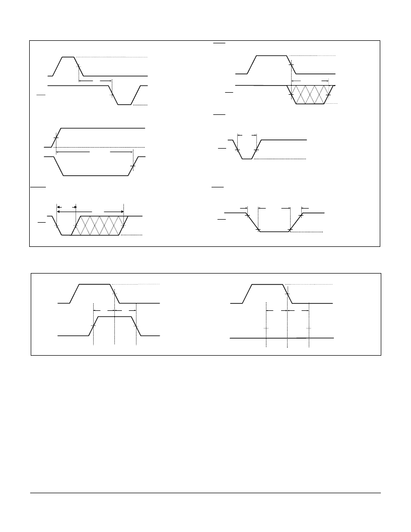
Figure 3. Timing Diagrams
Latency Timing
RxD Valid after Shutdown
LED Protection Timing
RxD Timing 1.2 and 4 Mbit/s Mode
RxD Timing, SIR mode. The output may be indeterminate
in the shaded area. Spurious transitions may occur.
RxD Rise and Fall Timing Measurements
Figure 4. Bandwidth Programming
Setting the Receiver to High BW Mode (FIR)
Setting the Receiver to Low BW Mode (SIR & MIR)
TxD
RxD
t
L
V
IH
V
IL
V
OH
V
OL
50%
50%
RxD
SD/ Mode
50%
V
IH
V
IL
t
RXEN
50%
V
OH
V
OL
TxD
LEDC
t
LEDP
V
IH
V
IL
50%
50%
t
W
RxD
50%
VOH
VOL
RxD
t
W(max)
t
W(min)
V
OH
V
OL
50%
50%
90%
10%
t
PLH
t
PHL
V
OH
V
OL
RxD
t
SU
SD/ Mode
TxD
t
H
50%
50%
50%
V
IH
V
IL
V
IH
VIL
(Setting high bandwidth mode)
SD/ Mode
50%
50%
50%
V
IH
V
IL
VIL
TxD
(Setting low bandwidth mode)
t
SU
t
H
The transceiver powers on with the receiver in low bandwidth
mode. To enable high bandwidth mode, apply timings as
shown in the figure 7, to the SD/ Mode and the TxD inputs.
Note that the internal LED driver is disabled when SD/ Mode is
active and is not enabled until the next rising edge of TxD. This
ensures that the LED will not be active during bandwidth
adjustment. It is recommended that the SD/ Mode pin be con-
nected to GND if bandwidth adjustment and shutdown mode
are not used.
Setting the Receiver to High Bandwidth Mode (see Figure 4)
1. Set the SD/ Mode input to ’logic high’.
2. Set the TxD input to ’logic high’. Wait t
su
≥
10 ns.
3. Set the SD/ Mode to ’logic low’. (This high-to-low transition
latches the state of TxD, which determines the receiver
bandwidth.)
4. After waiting t
h
≥
10 ns, set the TxDinput to ’logic low’. The
receiver is in high bandwidth mode within 200
μ
s of the SD/
Mode rising edge or 10 ns after the SD/ Mode falling edge,
whichever occurs later.
Setting the Receiver to Low Bandwidth Mode (see Figure 4)
1. Set the SD/ Mode input to ’logic high’.
2. Ensure that the TxD input is at ’logic low’. Wait t
su
≥
10 ns.
3. Set the SD/ Mode to ’logic low’. (This high-to-low transition
latches the state of TxD, which determines the receiver
bandwidth.)
4. Ensure that the TxD input remains low for t
h
≥
10 ns. The
receiver is in low bandwidth mode within 200
μ
s of the SD/
Mode rising edge or 10 ns after the SD/ Mode falling edge,
whichever occurs later.
相关PDF资料 |
PDF描述 |
|---|---|
| IRMT6452 | SIDE VIEW IRMS6452/TOP VIEW |
| IS82C37A-12 | CMOS High Performance Programmable DMA Controller |
| IS82C37A | CMOS High Performance Programmable DMA Controller |
| IS82C37A-5 | CMOS High Performance Programmable DMA Controller |
| IS82C37A-12 | SCHOTTKY 30V DIODE SOT23 COMMON CATHODE |
相关代理商/技术参数 |
参数描述 |
|---|---|
| IRMS6453 | 制造商:INFINEON 制造商全称:Infineon Technologies AG 功能描述:4 Mb/s Infrared Data Transceiver |
| IRMT6400 | 制造商:未知厂家 制造商全称:未知厂家 功能描述:FIBER OPTIC TRANSCEIVER |
| IRMT6452 | 制造商:VISHAY 制造商全称:Vishay Siliconix 功能描述:SIDE VIEW IRMS6452/TOP VIEW |
| IRM-V036/TR1 | 制造商:EVERLIGHT 制造商全称:Everlight Electronics Co., Ltd 功能描述:Infrared Remote-control Receiver Module |
| IRM-V036-TR1 | 制造商:EVERLIGHT 制造商全称:Everlight Electronics Co., Ltd 功能描述:Infrared Remote-control Receiver Module |
发布紧急采购,3分钟左右您将得到回复。