- 您现在的位置:买卖IC网 > PDF目录17556 > IRS2117STRPBF (International Rectifier)IC DRIVER SGL CHAN 8-SOIC PDF资料下载
参数资料
| 型号: | IRS2117STRPBF |
| 厂商: | International Rectifier |
| 文件页数: | 12/26页 |
| 文件大小: | 0K |
| 描述: | IC DRIVER SGL CHAN 8-SOIC |
| 标准包装: | 2,500 |
| 配置: | 高端 |
| 输入类型: | 非反相 |
| 延迟时间: | 125ns |
| 电流 - 峰: | 290mA |
| 配置数: | 1 |
| 输出数: | 1 |
| 高端电压 - 最大(自引导启动): | 600V |
| 电源电压: | 10 V ~ 20 V |
| 工作温度: | -40°C ~ 125°C |
| 安装类型: | 表面贴装 |
| 封装/外壳: | 8-SOIC(0.154",3.90mm 宽) |
| 供应商设备封装: | 8-SOIC |
| 包装: | 带卷 (TR) |
�� �
�
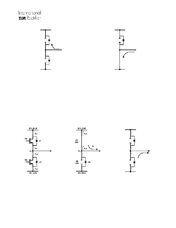
�IRS211(7,71,8)(S)�
�DC+� BUS�
�DC+� BUS�
�Q1�
�OFF�
�D1�
�Q1�
�OFF�
�D1�
�I� L�
�V� S�
�V� S�
�I� L�
�Q2�
�OFF�
�D2�
�Q2�
�ON�
�DC-� BUS�
�Figure� 8:� D1� conducting�
�DC-� BUS�
�Figure� 9:� Q2� conducting�
�However,� in� a� real� inverter� circuit,� the� V� S� voltage� swing� does� not� stop� at� the� level� of� the� negative� DC� bus,�
�rather� it� swings� below� the� level� of� the� negative� DC� bus.� This� undershoot� voltage� is� called� “negative� V� S�
�transient”.�
�The� circuit� shown� in� Figure� 10� depicts� a� half� bridge� circuit� with� parasitic� elements� shown;� Figures� 11� and� 12�
�show� a� simplified� illustration� of� the� commutation� of� the� current� between� Q1� and� D2.� The� parasitic� inductances�
�in� the� power� circuit� from� the� die� bonding� to� the� PCB� tracks� are� lumped� together� in� L� D� and� L� S� for� each� switch.�
�When� the� high-side� switch� is� on,� V� S� is� below� the� DC+� voltage� by� the� voltage� drops� associated� with� the� power�
�switch� and� the� parasitic� elements� of� the� circuit.� When� the� high-side� power� switch� turns� off,� the� load� current� can�
�momentarily� flow� in� the� low-side� freewheeling� diode� due� to� the� inductive� load� connected� to� V� S� (the� load� is� not�
�shown� in� these� figures).� This� current� flows� from� the� DC-� bus� (which� is� connected� to� the� COM� pin� of� the� HVIC)�
�to� the� load� and� a� negative� voltage� between� V� S� and� the� DC-� Bus� is� induced� (i.e.,� the� COM� pin� of� the� HVIC� is� at�
�a� higher� potential� than� the� V� S� pin).�
�DC+� BUS�
�Q1�
�OFF�
�V� S�
�+�
�D1�
�Q2�
�OFF�
�_�
�+�
�_�
�V� LD2�
�V� LS2�
�D2�
�I� L�
�DC-� BUS�
�Figure� 10:� Parasitic� Elements�
�Figure� 11:� V� S� positive�
�Figure� 12:� V� S� negative�
�In� a� typical� power� circuit,� dV/dt� is� typically� designed� to� be� in� the� range� of� 1-5� V/ns.� The� negative� V� S� transient�
�voltage� can� exceed� this� range� during� some� events� such� as� short� circuit� and� over-current� shutdown,� when� di/dt�
�is� greater� than� in� normal� operation.�
�International� Rectifier’s� HVICs� have� been� designed� for� the� robustness� required� in� many� of� today’s� demanding�
�applications.� An� indication� of� the� IRS211(7,71,8)’s� robustness� can� be� seen� in� Figure� 13,� where� there� is�
�represented� the� IRS211(7,71,8)� Safe� Operating� Area� at� V� BS� =15V� based� on� repetitive� negative� V� S� spikes.� A�
�negative� V� S� transient� voltage� falling� in� the� grey� area� (outside� SOA)� may� lead� to� IC� permanent� damage;�
�viceversa� unwanted� functional� anomalies� or� permanent� damage� to� the� IC� do� not� appear� if� negative� Vs�
�transients� fall� inside� SOA.�
�www.irf.com�
�12�
�?� 2008� International� Rectifier�
�相关PDF资料 |
PDF描述 |
|---|---|
| T95X226M004HZAL | CAP TANT 22UF 4V 20% 2910 |
| IR4426PBF | IC DRIVER DUAL LOW SIDE 8-DIP |
| T95X226K6R3HZAL | CAP TANT 22UF 6.3V 10% 2910 |
| IR2102PBF | IC DRIVER HIGH/LOW SIDE 8-DIP |
| 3057Y-1-253 | TRIMMER 25K OHM 1W TH |
相关代理商/技术参数 |
参数描述 |
|---|---|
| IRS2118 | 制造商:IRF 制造商全称:International Rectifier 功能描述:SINGLE CHANNEL DRIVER |
| IRS2118PBF | 功能描述:功率驱动器IC Sngl Hi Sd Drvr Invrt Inpt RoHS:否 制造商:Micrel 产品:MOSFET Gate Drivers 类型:Low Cost High or Low Side MOSFET Driver 上升时间: 下降时间: 电源电压-最大:30 V 电源电压-最小:2.75 V 电源电流: 最大功率耗散: 最大工作温度:+ 85 C 安装风格:SMD/SMT 封装 / 箱体:SOIC-8 封装:Tube |
| IRS2118PBF | 制造商:International Rectifier 功能描述:MOSFET Driver IC |
| IRS2118SPbF | 功能描述:功率驱动器IC 1 NONINVERTING INPUT VTG THRESHOLD RoHS:否 制造商:Micrel 产品:MOSFET Gate Drivers 类型:Low Cost High or Low Side MOSFET Driver 上升时间: 下降时间: 电源电压-最大:30 V 电源电压-最小:2.75 V 电源电流: 最大功率耗散: 最大工作温度:+ 85 C 安装风格:SMD/SMT 封装 / 箱体:SOIC-8 封装:Tube |
| IRS2118SPBF | 制造商:International Rectifier 功能描述:MOSFET Driver IC |
发布紧急采购,3分钟左右您将得到回复。