- 您现在的位置:买卖IC网 > Datasheet目录333 > IRS21856SPBF (International Rectifier)IC DVR LOW SIDE/DUAL HI 14-SOIC Datasheet资料下载
参数资料
| 型号: | IRS21856SPBF |
| 厂商: | International Rectifier |
| 文件页数: | 8/21页 |
| 文件大小: | 0K |
| 描述: | IC DVR LOW SIDE/DUAL HI 14-SOIC |
| 标准包装: | 55 |
| 配置: | 高端和低端,同步 |
| 输入类型: | 非反相 |
| 延迟时间: | 150ns |
| 电流 - 峰: | 500mA |
| 配置数: | 1 |
| 输出数: | 2 |
| 高端电压 - 最大(自引导启动): | 600V |
| 电源电压: | 10 V ~ 20 V |
| 工作温度: | -40°C ~ 125°C |
| 安装类型: | 表面贴装 |
| 封装/外壳: | 14-SOIC(0.154",3.90mm 宽) |
| 供应商设备封装: | 14-SOIC |
| 包装: | 管件 |
�� �
�
�IRS21856S�
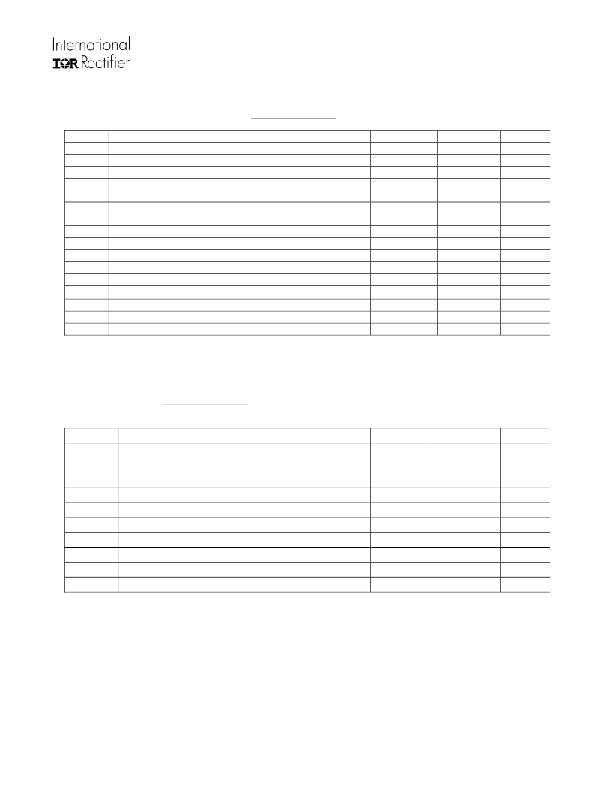
�Absolute� Maximum� Ratings�
�Absolute� maximum� ratings� indicate� sustained� limits� beyond� which� damage� to� the� device� may� occur.� All�
�voltage� parameters� are� absolute� voltages� referenced to COM� .�
�Symbol� Definition�
�Min�
�Max�
�Units�
�V� CC�
�V� IN�
�V� LO�
�V� DV� ,�
�V� VREF�
�V� VSE� ,�
�V� RES�
�V� B�
�V� S�
�V� HO1�
�Low� side� supply� voltage�
�Logic� input� voltage� (HIN1,� HIN2,� LIN3)�
�Low� side� gate� drive� output� voltage�
�High� side� inputs� voltage�
�High� side� inputs� voltage�
�High� side� floating� well� supply� voltage�
�High� side� floating� well� supply� return� voltage�
�Floating� gate� drive� output� voltage�
�-0.3�
�COM-0.3�
�COM-0.3�
�VS-0.3�
�VS-0.3�
�-0.3�
�VB-25�
�VS-0.3�
�25�
�VCC� +0.3�
�VCC� +0.3�
�VB+0.3�
�VB+0.3�
�625�
�VB+0.3�
�VB+0.3�
�V�
�V�
�V�
�V�
�V�
�V�
�V�
�V�
�dV� S� /dt� Allowable� VS� offset� supply� transient� relative� to� COM�
�-�
�50�
�V/ns�
�P� D�
�R� θ� JA�
�T� J�
�T� S�
�T� L�
�Package� Power� Dissipation� @� TA<=+25oC�
�Thermal� Resistance,� Junction� to� Ambient�
�Junction� Temperature�
�Storage� Temperature�
�Lead� temperature� (Soldering,� 10� seconds)�
�-�
�-�
�-55�
�-55�
�-�
�1.0�
�120�
�150�
�150�
�300�
�W�
�oC/W�
�oC�
�oC�
�oC�
�Recommended� Operating� Conditions�
�For� proper� operation,� the� device� should� be� used� within� the� recommended� conditions.� All� voltage� parameters�
�are� absolute� voltages� referenced to COM� .� The� offset� rating� are� tested� with� supplies� of� (VCC-COM)� =� (VB-�
�VS)=15V.�
�Symbol�
�V� CC�
�V� IN�
�V� LO3�
�V� B�
�V� RES�
�V� DV�
�V� VREF,� VSE�
�V� S�
�V� HO1�
�T� A�
�Definition�
�Low� side� supply� voltage�
�HIN1,� HIN2,� LIN3� input� voltage�
�Low� side� gate� drive� output� voltage�
�High� side� floating� well� supply� voltage�
�RES� input� voltage�
�DV� input� voltage�
�VREF� and� VSE� input� voltage�
�High� side� floating� well� supply� offset� voltage�
�Floating� gate� drive� output� voltage�
�Ambient� Temperature�
�Min�
�10�
�COM�
�COM�
�V� S� +10�
�V� S�
�V� S�
�V� S�
�Note2??�
�V� S�
�-40�
�Max�
�20�
�V� CC�
�V� CC�
�V� S� +20�
�V� B�
�V� B�
�V� B� -3�
�600�
�V� B�
�125�
�Units�
�V�
�V�
�V�
�V�
�V�
�V�
�V�
�V�
�V�
�oC�
�?�
�??�
�V� S� and� V� B� voltages� will� be� tolerant� to� short� negative� transient� spikes.� These� will� be� defined� and�
�specified� in� the� future.�
�Logic� operation� for� Vs� of� -5� to� 600V.� Logic� state� held� for� Vs� of� -5V� to� –V� BS� .� (Please� refer� to� Design� Tip�
�DT97-3� for� more� details).�
�www.irf.com�
�8�
�?� 2008� International� Rectifier�
�相关PDF资料 |
PDF描述 |
|---|---|
| IRS21858SPBF | IC DVR LOW SIDE/DUAL HI 16-SOIC |
| IRS21864STRPBF | IC DRIVER HI/LO SIDE 600V 14SOIC |
| IRS21867SPBF | IC MOSFET DRIVER |
| IRS21952SPBF | IC DVR HISIDE DUAL LOSIDE 16SOIC |
| IRS21953SPBF | IC DVR HISIDE DUAL LOSIDE 16SOIC |
相关代理商/技术参数 |
参数描述 |
|---|---|
| IRS21856STRPBF | 功能描述:功率驱动器IC Ramp Slope Cntrl Driver Hi Volt RoHS:否 制造商:Micrel 产品:MOSFET Gate Drivers 类型:Low Cost High or Low Side MOSFET Driver 上升时间: 下降时间: 电源电压-最大:30 V 电源电压-最小:2.75 V 电源电流: 最大功率耗散: 最大工作温度:+ 85 C 安装风格:SMD/SMT 封装 / 箱体:SOIC-8 封装:Tube |
| IRS21858SPBF | 功能描述:功率驱动器IC Hig Dual Side DRVR 600V 290mA 160ns RoHS:否 制造商:Micrel 产品:MOSFET Gate Drivers 类型:Low Cost High or Low Side MOSFET Driver 上升时间: 下降时间: 电源电压-最大:30 V 电源电压-最小:2.75 V 电源电流: 最大功率耗散: 最大工作温度:+ 85 C 安装风格:SMD/SMT 封装 / 箱体:SOIC-8 封装:Tube |
| IRS21858STRPBF | 功能描述:功率驱动器IC Hi&Lw Sd Dual Drvr IC RoHS:否 制造商:Micrel 产品:MOSFET Gate Drivers 类型:Low Cost High or Low Side MOSFET Driver 上升时间: 下降时间: 电源电压-最大:30 V 电源电压-最小:2.75 V 电源电流: 最大功率耗散: 最大工作温度:+ 85 C 安装风格:SMD/SMT 封装 / 箱体:SOIC-8 封装:Tube |
| IRS2186 | 制造商:IRF 制造商全称:International Rectifier 功能描述:HIGH AND LOW SIDE DRIVER |
| IRS21864PBF | 功能描述:功率驱动器IC Hi&Lw Sd Drvr capbl of 4A & 4A RoHS:否 制造商:Micrel 产品:MOSFET Gate Drivers 类型:Low Cost High or Low Side MOSFET Driver 上升时间: 下降时间: 电源电压-最大:30 V 电源电压-最小:2.75 V 电源电流: 最大功率耗散: 最大工作温度:+ 85 C 安装风格:SMD/SMT 封装 / 箱体:SOIC-8 封装:Tube |
发布紧急采购,3分钟左右您将得到回复。