- 您现在的位置:买卖IC网 > PDF目录381957 > ISB35166 (意法半导体) GT 48C 48#16 PIN PLUG PDF资料下载
参数资料
| 型号: | ISB35166 |
| 厂商: | 意法半导体 |
| 英文描述: | GT 48C 48#16 PIN PLUG |
| 中文描述: | HCMOS结构化阵列 |
| 文件页数: | 14/15页 |
| 文件大小: | 345K |
| 代理商: | ISB35166 |
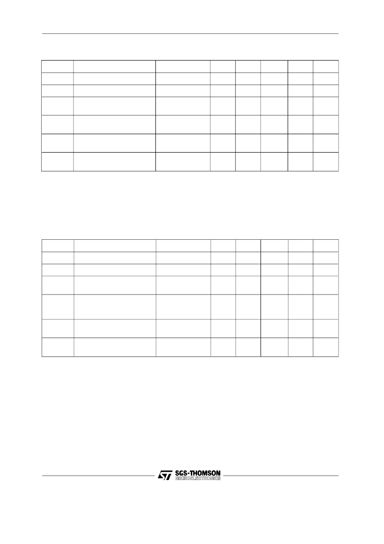
Symbol
Parameter
Conditions
Min
Typ
Max
Unit
Notes
V
IL
Low Level Input Voltage
0.8
Volts
2,3
V
IH
High Level Input Voltage
2.0
Volts
2,3
V
OL
Low Level Output Voltage
I
OL
= Rated Buffer
Current
0.2
0.4
Volts
2,3,4
V
OH
High Level Output Voltage
I
OH
= Rated Buffer
Current
2.4
3.0
Volts
2,3,4
V
t +
Schmitt Trigger +Ve
Threshold
1.7
1.9
Volts
2,3
V
t -
Schmitt Trigger -Ve
Threshold
0.9
1.1
Volts
2,3
Note 1
. These are normal Voltage and extended temperature specifications V
DD
from 3.0 V to 3.6 V
Temperature Ambient from -55 to 125 degrees Centigrade
Note 2
. Adherence to rules in Power Pin / Pad Specifications Required
Note 3
. Refer to the ISB35000 Gate Array Specification for full Testing Levels and Conditions
Note 4
. Buffers offered in 2, 4, 8, 12, 16, and 24 mA TTL options
Table 9. LVTTL Interface DC Electrical Characteristics (Note 1)
Symbol
Parameter
Conditions
Min
Typ
Max
Unit
Notes
V
IL
Low Level Input Voltage
0.2xV
DD
Volts
2,3,4
V
IH
High Level Input Voltage
0.8xV
DD
Volts
2,3,4
V
OL
Low Level Output Voltage
I
OL
= Rated Buffer
Current
0.2
0.4
Volts
2,3,4,5,6
V
OH
High Level Output Voltage
I
OH
= Rated Buffer
Current
0.85
x
V
DD
0.9
x
V
DD
Volts
2,3,4,5,6
V
t +
Schmitt Trigger +Ve
Threshold
1.7
1.9
Volts
2,3
V
t -
Schmitt Trigger -Ve
Threshold
0.9
1.1
Volts
2,3
Note 1
. These are extended voltage and temperature specifications
V
from 2.7 V to 3.6 V
Temperature Ambient from -55 to 125 degrees Centigrade
Note 2
. Adherence to rules in Power Pin / Pad Specifications Required
Note 3
. Refer to the ISB35000 Gate Array Specification for full Testing Levels and Conditions
Note 4
. Buffers offered in 2, 4, and 8 mA CMOS options
Note 5
. Note only one CMOS buffer may sink or source DC current when parametric measurements are taken due to the reason that the power
supply specifications for CMOS product are not written to support DC current. If more than one buffer is active voltage drops in the
supply may cause false failure readings.
Note 6
. If no buffers are sinking or sourcing current and all internal pull up or pull down resistors in bidi buffers have been disabled by having
the T2 Test Pin positive V
OL
(max) = 0.05 Volts and V
OH
(min)=V
DD
-0.05 Volts
Table 10. LVCMOS Interface DC Electrical Characteristics (Note 1)
ISB35000 SERIES
14/15
相关PDF资料 |
PDF描述 |
|---|---|
| ISB35208 | GT 48C 48#16 PIN PLUG |
| ISB35389 | HCMOS STRUCTURED ARRAY |
| ISB35484 | HCMOS STRUCTURED ARRAY |
| ISB35666 | HCMOS STRUCTURED ARRAY |
| ISB35832 | HCMOS STRUCTURED ARRAY |
相关代理商/技术参数 |
参数描述 |
|---|---|
| ISB35208 | 制造商:STMICROELECTRONICS 制造商全称:STMicroelectronics 功能描述:HCMOS STRUCTURED ARRAY |
| ISB35279 | 制造商:STMICROELECTRONICS 制造商全称:STMicroelectronics 功能描述:HCMOS STRUCTURED ARRAY |
| ISB35389 | 制造商:STMICROELECTRONICS 制造商全称:STMicroelectronics 功能描述:HCMOS STRUCTURED ARRAY |
| ISB35484 | 制造商:STMICROELECTRONICS 制造商全称:STMicroelectronics 功能描述:HCMOS STRUCTURED ARRAY |
| ISB35666 | 制造商:STMICROELECTRONICS 制造商全称:STMicroelectronics 功能描述:HCMOS STRUCTURED ARRAY |
发布紧急采购,3分钟左右您将得到回复。