参数资料
| 型号: | ISL12027IBAZ |
| 厂商: | Intersil |
| 文件页数: | 6/28页 |
| 文件大小: | 0K |
| 描述: | IC RTC/CALENDAR EEPROM 8-SOIC |
| 产品培训模块: | Solutions for Industrial Control Applications |
| 标准包装: | 980 |
| 类型: | 时钟/日历 |
| 特点: | 警报器,闰年,监控器,监视计时器 |
| 时间格式: | HH:MM:SS(12/24 小时) |
| 数据格式: | YY-MM-DD-dd |
| 接口: | I²C,2 线串口 |
| 电源电压: | 2.7 V ~ 5.5 V |
| 电压 - 电源,电池: | 1.8 V ~ 5.5 V |
| 工作温度: | -40°C ~ 85°C |
| 安装类型: | 表面贴装 |
| 封装/外壳: | 8-SOIC(0.154",3.90mm 宽) |
| 供应商设备封装: | 8-SOIC |
| 包装: | 管件 |
第1页第2页第3页第4页第5页当前第6页第7页第8页第9页第10页第11页第12页第13页第14页第15页第16页第17页第18页第19页第20页第21页第22页第23页第24页第25页第26页第27页第28页
14
FN8232.8
August 12, 2010
PWR Register: SBIB, BSW, VTS2, VTS1, VTS0
SBIB: Serial Bus Interface (Enable)
The serial bus can be disabled in battery backup mode by
setting this bit to “1”. This will minimize power drain on the
battery. The Serial Interface can be enabled in battery
backup mode by setting this bit to “0” (default is “0”). See
“Power Control Operation” on page 15 and “RESET” on
page 9.
BSW: Power Control Bit
The Power Control bit, BSW, determines the conditions for
switching between VDD and Backup Battery. There are two
options:
Option 1. Standard: Set “BSW = 0” (default for ISL12027A)
Option 2. Legacy /Default Mode: Set “BSW = 1” (default
for ISL12027)
See “Power Control Operation” on page 15 for more details.
Also see “I2C Communications During Battery Backup and
LVR Operation” on page 24 for important details.
VTS2, VTS1, VTS0: VRESET Select Bits
The ISL12027 is shipped with a default VDD threshold
(VRESET) per the “Ordering Information” table on page 2.
This register is a non-volatile with no protection, therefore
any writes to this location can change the default value from
that marked on the package. If not changed with a non-
volatile write, this value will not change over normal
operating and storage conditions. However, ISL12027 has
four (4) additional selectable levels to fit the customers
application. Levels are: 4.64V (default), 4.38V, 3.09V, 2.92V
and 2.63V. The VRESET selection is via 3 bits (VTS2, VTS1
and VTS0). See Table 5.
Care should be taken when changing the VRESET select bits.
If the VRESET voltage selected is higher than VDD, then the
device will go into RESET and unless VDD is increased, the
device will no longer be able to communicate using the I2C
bus.
In battery mode, the RESET signal output is asserted LOW
when the VDD voltage supply has dipped below the VRESET
threshold, but the RESET signal output will not return HIGH
until the device is back to VDD mode even the VDD voltage is
above VRESET threshold.
Device Operation
Writing to the Clock/Control Registers
Changing any of the bits of the clock/control registers
requires the following steps:
1. Write a 02h to the Status Register to set the Write Enable
Latch (WEL). This is a volatile operation, so there is no
delay after the write. (Operation preceded by a start and
ended with a stop).
2. Write a 06h to the Status Register to set both the Register
Write Enable Latch (RWEL) and the WEL bit. This is also
a volatile cycle. The zeros in the data byte are required.
(Operation proceeded by a start and ended with a stop).
Write all 8 bytes to the RTC registers, or one byte to the SR,
or one to five bytes to the control registers. This sequence
starts with a start bit, requires a slave byte of “11011110” and
an address within the CCR and is terminated by a stop bit. A
write to the EEPROM registers in the CCR will initiate a
non-volatile write cycle and will take up to 20ms to complete.
A write to the RTC registers (SRAM) will require much
shorter cycle time (t = tBUF). Writes to undefined areas have
no effect. The RWEL bit is reset by the completion of a write
to the CCR, so the sequence must be repeated to again
initiate another change to the CCR contents. If the sequence
is not completed for any reason (by sending an incorrect
number of bits or sending a start instead of a stop, for
example) the RWEL bit is not reset and the device remains
in an active mode. Writing all zeros to the status register
resets both the WEL and RWEL bits. A read operation
occurring between any of the previous operations will not
interrupt the register write operation.
Alarm Operation
Since the alarm works as a comparison between the alarm
registers and the RTC registers, it is ideal for notifying a host
processor of a particular time event and trigger some action as
a result. The host can be notified by polling the Status Register
(SR) Alarm bits. These two volatile bits (AL1 for Alarm 1 and
AL0 for Alarm 0), indicate if an alarm has happened. The AL1
and AL0 bits in the status register are reset by the falling edge
of the eighth clock of status register read.
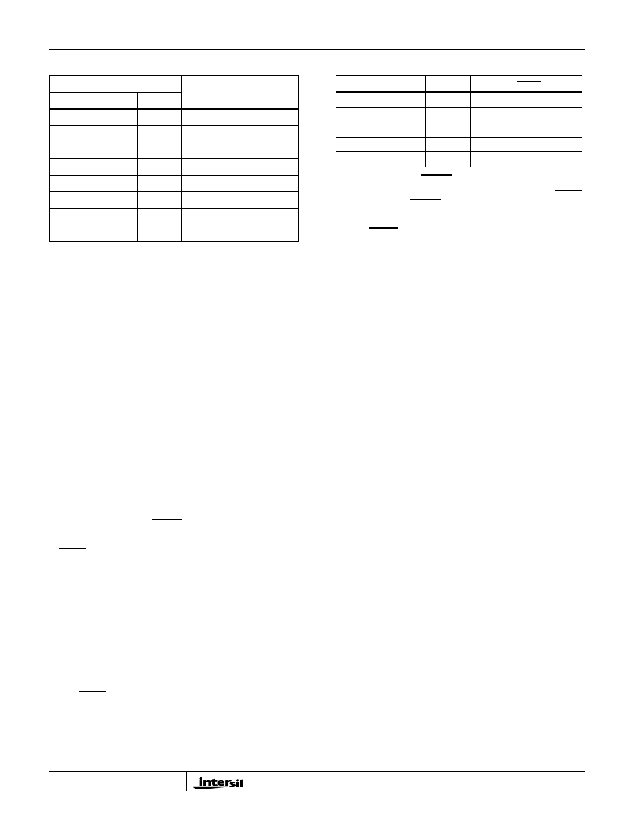
TABLE 4. DIGITAL TRIMMING REGISTERS
DTR REGISTER
ESTIMATED FREQUENCY
PPM
DTR2
DTR1
DTR0
00
0
01
0
+10
00
1
+20
01
1
+30
10
0
11
0
-10
10
1
-20
11
1
-30
TABLE 5.
VTS2
VTS1
VTS0
VRESET
0
4.64V
0
1
4.38V
0
1
0
3.09V
0
1
2.92V
1
0
2.63V
ISL12027, ISL12027A
相关PDF资料 |
PDF描述 |
|---|---|
| ISL12027IB30AZ | IC RTC/CALENDAR EEPROM 8-SOIC |
| ISL12027IBZ | IC RTC/CAL W/EEPROM 8-SOIC |
| ISL12027IB27Z | IC RTC/CAL W/EEPROM 2.7V 8-SOIC |
| ISL12029IV30AZ-T | IC RTC/CALENDAR EEPROM 14-TSSOP |
| ISL12028IVAZ-T | IC RTC/CALENDAR EEPROM 14-TSSOP |
相关代理商/技术参数 |
参数描述 |
|---|---|
| ISL12027IBAZR5328 | 制造商:Rochester Electronics LLC 功能描述: 制造商:Intersil Corporation 功能描述: |
| ISL12027IBAZ-T | 功能描述:实时时钟 REAL TIME CLK/CLNDR W/EEPROM 4 64VSET RoHS:否 制造商:Microchip Technology 功能:Clock, Calendar. Alarm RTC 总线接口:I2C 日期格式:DW:DM:M:Y 时间格式:HH:MM:SS RTC 存储容量:64 B 电源电压-最大:5.5 V 电源电压-最小:1.8 V 最大工作温度:+ 85 C 最小工作温度: 安装风格:Through Hole 封装 / 箱体:PDIP-8 封装:Tube |
| ISL12027IBZ | 功能描述:实时时钟 REAL TIME CLK/CLNDR W/EEPROM IN 8LD RoHS:否 制造商:Microchip Technology 功能:Clock, Calendar. Alarm RTC 总线接口:I2C 日期格式:DW:DM:M:Y 时间格式:HH:MM:SS RTC 存储容量:64 B 电源电压-最大:5.5 V 电源电压-最小:1.8 V 最大工作温度:+ 85 C 最小工作温度: 安装风格:Through Hole 封装 / 箱体:PDIP-8 封装:Tube |
| ISL12027IBZ-T | 功能描述:实时时钟 REAL TIME CLK/CLNDR W/EEPROM IN 8LD RoHS:否 制造商:Microchip Technology 功能:Clock, Calendar. Alarm RTC 总线接口:I2C 日期格式:DW:DM:M:Y 时间格式:HH:MM:SS RTC 存储容量:64 B 电源电压-最大:5.5 V 电源电压-最小:1.8 V 最大工作温度:+ 85 C 最小工作温度: 安装风格:Through Hole 封装 / 箱体:PDIP-8 封装:Tube |
| ISL12027IV27AZ | 功能描述:实时时钟 REAL TIME CLK/CLNDR W/EEPROM 2 92VSET RoHS:否 制造商:Microchip Technology 功能:Clock, Calendar. Alarm RTC 总线接口:I2C 日期格式:DW:DM:M:Y 时间格式:HH:MM:SS RTC 存储容量:64 B 电源电压-最大:5.5 V 电源电压-最小:1.8 V 最大工作温度:+ 85 C 最小工作温度: 安装风格:Through Hole 封装 / 箱体:PDIP-8 封装:Tube |
发布紧急采购,3分钟左右您将得到回复。