- 您现在的位置:买卖IC网 > PDF目录383128 > ISL1208 (Intersil Corporation) I2C Real Time Clock/Calendar(I2C实时时钟/日历) PDF资料下载
参数资料
| 型号: | ISL1208 |
| 厂商: | Intersil Corporation |
| 英文描述: | I2C Real Time Clock/Calendar(I2C实时时钟/日历) |
| 中文描述: | 的I2C实时时钟/日历(的I2C实时时钟/日历) |
| 文件页数: | 4/21页 |
| 文件大小: | 349K |
| 代理商: | ISL1208 |
4
FN8085.5
August 23, 2006
Cpin
SDA and SCL Pin Capacitance
T
A
= 25°C, f = 1MHz, V
DD
= 5V,
V
IN
= 0V, V
OUT
= 0V
10
pF
f
SCL
SCL Frequency
400
kHz
t
IN
Pulse width Suppression Time at SDA
and SCL Inputs
Any pulse narrower than the max spec
is suppressed.
50
ns
t
AA
SCL Falling Edge to SDA Output Data
Valid
SCL falling edge crossing 30% of V
DD
,
until SDA exits the 30% to 70% of V
DD
window.
900
ns
t
BUF
Time the Bus Must Be Free Before the
Start of a New Transmission
SDA crossing 70% of V
DD
during a
STOP condition, to SDA crossing 70%
of V
DD
during the following START
condition.
1300
ns
t
LOW
Clock LOW Time
Measured at the 30% of V
DD
crossing.
1300
ns
t
HIGH
Clock HIGH Time
Measured at the 70% of V
DD
crossing.
600
ns
t
SU:STA
START Condition Setup Time
SCL rising edge to SDA falling edge.
Both crossing 70% of V
DD
.
600
ns
t
HD:STA
START Condition Hold Time
From SDA falling edge crossing 30% of
V
DD
to SCL falling edge crossing 70%
of V
DD
.
600
ns
t
SU:DAT
Input Data Setup Time
From SDA exiting the 30% to 70% of
V
DD
window, to SCL rising edge
crossing 30% of V
DD
100
ns
t
HD:DAT
Input Data Hold Time
From SCL falling edge crossing 30% of
V
DD
to SDA entering the 30% to 70%
of V
DD
window.
20
900
ns
t
SU:STO
STOP Condition Setup Time
From SCL rising edge crossing 70% of
V
DD
, to SDA rising edge crossing 30%
of V
DD
.
600
ns
t
HD:STO
STOP Condition Hold Time
From SDA rising edge to SCL falling
edge. Both crossing 70% of V
DD
.
600
ns
t
DH
Output Data Hold Time
From SCL falling edge crossing 30% of
V
DD
, until SDA enters the 30% to 70%
of V
DD
window.
0
ns
t
R
SDA and SCL Rise Time
From 30% to 70% of V
DD
20 +
0.1 x Cb
300
ns
t
F
SDA and SCL Fall Time
From 70% to 30% of V
DD
20 +
0.1 x Cb
300
ns
Cb
Capacitive Loading of SDA or SCL
Total on-chip and off-chip
10
400
pF
Rpu
SDA and SCL Bus Pull-Up Resistor
Off-Chip
Maximum is determined by t
R
and t
F
.
For Cb = 400pF, max is about 2~2.5k
.
For Cb = 40pF, max is about 15~20k
1
k
NOTES:
1. IRQ & F
OUT
Inactive.
2. LPMODE = 0 (default).
3. In order to ensure proper timekeeping, the V
DD SR-
specification must be followed.
4. Typical values are for T = 25°C and 3.3V supply voltage.
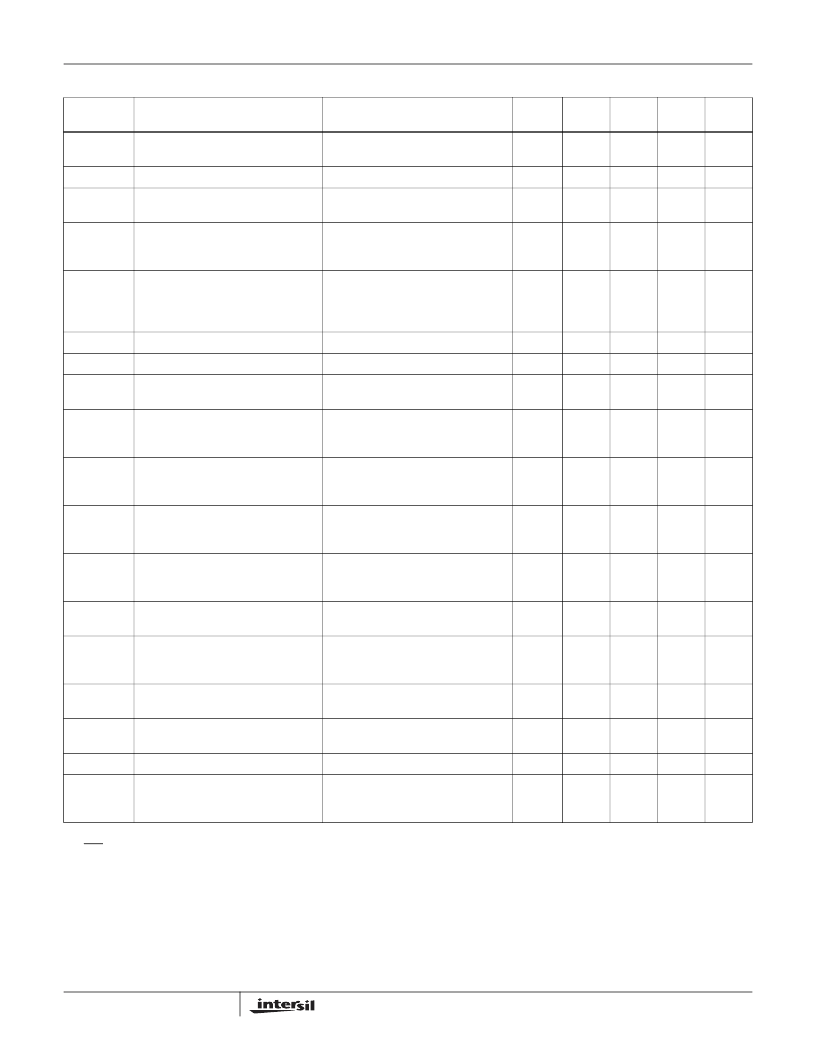
Serial Interface Specifications
Over the recommended operating conditions unless otherwise specified.
(Continued)
SYMBOL
PARAMETER
TEST CONDITIONS
MIN
TYP
(Note 4)
MAX
UNITS
NOTES
ISL1208
相关PDF资料 |
PDF描述 |
|---|---|
| ISL1218 | Low Power RTC with Battery Backed SRAM(具有电池供电SRAM的低功率RTC) |
| ISL1219 | Low Power RTC with Battery Backed SRAM and Event Detection(具有电池供电的SRAM和事件检测功能的低功率RTC) |
| ISL1220 | Low Power RTC with 8 Bytes of Battery Backed SRAM and Separate FOUT(具有电池供电的8位SRAM和独立输出的低功率RTC) |
| ISL1221 | Low Power RTC with Battery Backed SRAM and Event Detection(具有电池供电的SRAM和事件检测功能的低功率RTC) |
| ISL21009 | High Voltage Input Precision, Low Noise FGA Voltage References(高电压输入精度,低噪声FGA电压基准) |
相关代理商/技术参数 |
参数描述 |
|---|---|
| ISL1208_06 | 制造商:INTERSIL 制造商全称:Intersil Corporation 功能描述:Low Power RTC with Battery Backed SRAM |
| ISL12082 | 制造商:INTERSIL 制造商全称:Intersil Corporation 功能描述:I2C-Bus? Real Time Clock with Two Interrupts, Alarm, and Timer |
| ISL12082IB8Z | 功能描述:实时时钟 LW PWR RTC W/ALARM & TIMR FUNCTIONS 8LD RoHS:否 制造商:Microchip Technology 功能:Clock, Calendar. Alarm RTC 总线接口:I2C 日期格式:DW:DM:M:Y 时间格式:HH:MM:SS RTC 存储容量:64 B 电源电压-最大:5.5 V 电源电压-最小:1.8 V 最大工作温度:+ 85 C 最小工作温度: 安装风格:Through Hole 封装 / 箱体:PDIP-8 封装:Tube |
| ISL12082IB8Z-T | 功能描述:实时时钟 LW PWR RTC W/ALARM & TIMR FUNCTIONS 8LD RoHS:否 制造商:Microchip Technology 功能:Clock, Calendar. Alarm RTC 总线接口:I2C 日期格式:DW:DM:M:Y 时间格式:HH:MM:SS RTC 存储容量:64 B 电源电压-最大:5.5 V 电源电压-最小:1.8 V 最大工作温度:+ 85 C 最小工作温度: 安装风格:Through Hole 封装 / 箱体:PDIP-8 封装:Tube |
| ISL12082IUZ | 功能描述:实时时钟 RTC W/RESEAL ALARM & TIMR FUNCTNS IN MSO RoHS:否 制造商:Microchip Technology 功能:Clock, Calendar. Alarm RTC 总线接口:I2C 日期格式:DW:DM:M:Y 时间格式:HH:MM:SS RTC 存储容量:64 B 电源电压-最大:5.5 V 电源电压-最小:1.8 V 最大工作温度:+ 85 C 最小工作温度: 安装风格:Through Hole 封装 / 箱体:PDIP-8 封装:Tube |
发布紧急采购,3分钟左右您将得到回复。