参数资料
| 型号: | ISL1532IRZ |
| 厂商: | Intersil |
| 文件页数: | 8/19页 |
| 文件大小: | 0K |
| 描述: | IC LINE DRIVER DUAL 24-QFN |
| 标准包装: | 90 |
| 类型: | 驱动器 |
| 驱动器/接收器数: | 2/0 |
| 规程: | DSL |
| 电源电压: | 5 V ~ 15 V |
| 安装类型: | 表面贴装 |
| 封装/外壳: | 24-VFQFN 裸露焊盘 |
| 供应商设备封装: | 24-QFN(5x4) |
| 包装: | 散装 |
| 其它名称: | Q3116466 |
16
FN6173.3
December 4, 2006
The ISL1532 features improved frequency compensation for
all power modes and applications, allowing stable operation
at very low power levels and eliminating any need for
external "snubber" circuits. Differential circuits, such as
ADSL2+ line driver applications, can be especially prone to
common-mode oscillation. The ISL1532 is specifically
compensated to eliminate this type of instability and allow for
reliable operation even at very low power levels.
Cable Termination Techniques
The traditional circuit for a line driver with passive
resistance added for proper termination at the source. This
backmatch resistance is typically equal to the value of the
cable line characteristic impedance and the load impedance.
The output impedance of the amplifier is negligible in
comparison with the value of the backmatch resistor it
appears in series with. The gain equation reflects the output
voltage across the load resistance with respect to the input
voltage.
While functional, this passive termination circuit has some
disadvantages. The output impedance of the driver, while
small, can be a noticeable quantity. The backmatch resistor
is necessary to properly terminate the source end of a
transmission line such as a twisted pair, but now the voltage
delivered to the load is split between that backmatch
resistance and the load resistance. Since there is a required
voltage level at the load, the driver must now produce twice
the voltage swing. The voltage swing and power dissipation
increases. The power burned in the backmatch resistor is
lost as heat which causes the total power dissipation to
doubled. There also is quiescent power used in the op amp.
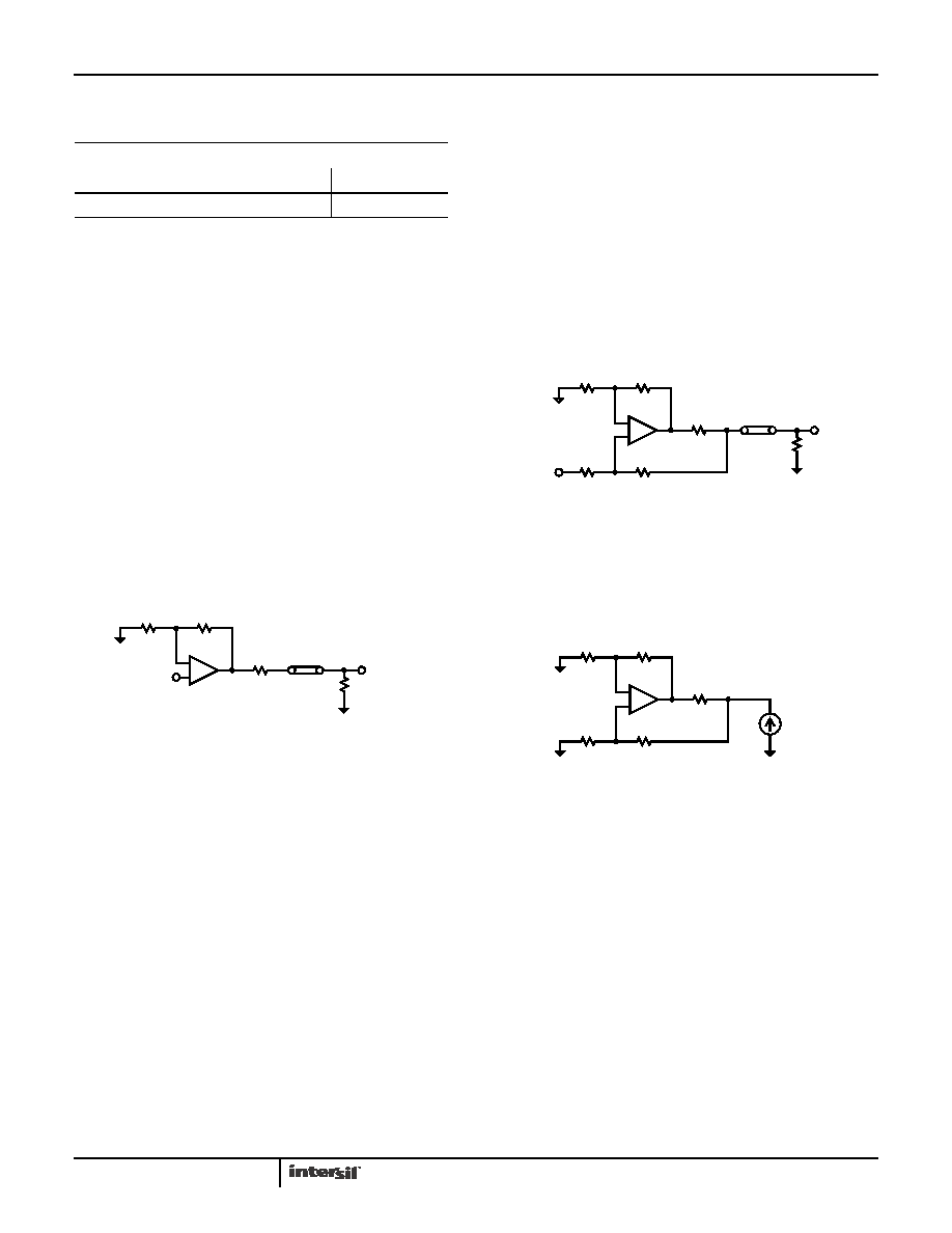
An alternative technique of cable termination using positive
feedback is shown in Figure 50. With negative feedback
already in place to set the gain, positive feedback can be
used to adjust the output impedance. Lowering the
backmatch resistor without compromising the total source
termination impedance relaxes the output and supply
voltage requirement for the amplifier and reduces the overall
power dissipation. RP1 and RP2 are the only additions to the
passive circuit and provide the positive feedback for the
amplifier. This feedback synthesizes larger output
impedance for the amplifier, allowing a reduction of the
backmatch resistance. For convenience, a factor K is being
introduced. It is the ratio between the backmatch resistance
and the physical backmatch resistor.
The stability of the amplifier and the physical backmatch
resistance tolerance typically limit K to around 4 or 5. The
output impedance of the amplifier is increased by the
positive feedback, allowing the backmatch resistance to
decrease-keeping the total source impedance constant.
Figure 51 shows a standard method for measuring the
output impedance of any circuit. Ohm's law applies, so a
measured voltage (VX) applied to a node divided by the test
current gives the impedance seen at that node. Ideal op amp
simplifications (input terminals are at the same voltage and
there is no current flowing into the inputs) RP2 is assumed
much larger the RBM so the current through the positive
feedback loop can be neglected. The voltage at the input
terminals is given by a resistive divider of the output voltage
on either side of the backmatch resistor. These feedback
resistors alter the output resistance for the op amp, allowing
reduction in the backmatch resistance. The derivations are
as follows:
TABLE 2. OPTIMUM DRIVER FEEDBACK RESISTOR FOR
VARIOUS GAINS AND SUPPLY VOLTAGES
SUPPLY VOLTAGE
DRIVER VOLTAGE GAIN
510
±12V
4k
3k
-
+
RF
RG
VIN
RBM
ZL
RL
VO
V
O
V
IN
---------
1
R
F
R
G
--------
+
R
L
R
BM
R
L
+
--------------------------
×
=
FIGURE 49. TRADITIONAL CABLE TERMINATION TECHNIQUE
K
R
L
RBM
--------------
=
(EQ. 8)
-
+
RF
RG
VIN
RBM
ZL
RL
VO
RP2
RP1
FIGURE 50. ACTIVE TERMINATION TECHNIQUE
-
+
RF
RG
RBM
VX
RP2
RP1
IX
FIGURE 51. MEASURING OUTPUT IMPEDANCE
ISL1532
相关PDF资料 |
PDF描述 |
|---|---|
| ISL1536IRZ | IC LINE DRVR DUAL ADSL2+ 16-QFN |
| ISL1539AIRZ | IC VDSL2 LINE DVR AMP 24QFN |
| ISL1539IVEZ | IC VDSL2 LINE DVR AMP 24HTTSOP |
| ISL1557AIRZ | IC LINE DRIVER DUAL 16-QFN |
| ISL1557IUEZ | IC VDSL2 LINE DVR AMP 10HMSOP |
相关代理商/技术参数 |
参数描述 |
|---|---|
| ISL1532IRZ-T13 | 制造商:Intersil Corporation 功能描述:ADSL DRVR DUAL 24QFN EP - Tape and Reel |
| ISL1532IRZ-T7 | 功能描述:缓冲器和线路驱动器 Dual Channel Diff. DSL Line Driver RoHS:否 制造商:Intersil 输入线路数量: 输出线路数量: 极性: 电源电压-最大: 电源电压-最小: 最大工作温度:+ 85 C 安装风格: 封装 / 箱体:QFN EP 封装:Reel |
| ISL1532IVEZ | 制造商:Intersil Corporation 功能描述:OP AMP DUAL CURRENT FDBK 15V 20HTSSOP - Bulk 制造商:Rochester Electronics LLC 功能描述: |
| ISL1532IVEZ-EVAL | 制造商:Intersil Corporation 功能描述:ISL1532IVEZ-EVAL DEMO BOARD - Bulk |
| ISL1532IVEZ-T13 | 制造商:Intersil Corporation 功能描述:ADSL DRVR DUAL 20HTSSOP EP - Tape and Reel 制造商:Intersil Corporation 功能描述:Dual Channel Differential DSL Line Drive |
发布紧急采购,3分钟左右您将得到回复。