- 您现在的位置:买卖IC网 > PDF目录16992 > ISL21010DFH312Z-TK (Intersil)IC INTERFACE PDF资料下载
参数资料
| 型号: | ISL21010DFH312Z-TK |
| 厂商: | Intersil |
| 文件页数: | 18/20页 |
| 文件大小: | 0K |
| 描述: | IC INTERFACE |
| 标准包装: | 1,000 |
| 系列: | * |
�� �
�
�ISL21010�
�Applications� Information�
�Micropower� Operation�
�The� ISL21010� consumes� very� low� supply� current� due� to� the�
�proprietary� bandgap� technology.� Low� noise� performance� is�
�achieved� using� optimized� biasing� techniques.� Supply� current� is�
�typically� 48μA� and� noise� in� the� 0.1Hz� to� 10Hz� bandwidth� is�
�58μV� P-P� to� 100μV� P-P� (V� OUT� =� 2.048V,� 3.0V,� and� 3.3V)� benefitting�
�precision,� low� noise� portable� applications� such� as� handheld�
�meters� and� instruments.�
�Data� Converters� in� particular� can� utilize� the� ISL21010� as� an�
�external� voltage� reference.� Low� power� DAC� and� ADC� circuits� will�
�realize� maximum� resolution� with� lowest� noise.� The� device�
�Maintains� output� voltage� during� conversion� cycles� with� fast�
�response,� although� it� is� helpful� to� add� an� output� capacitor,�
�typically� 1μF.�
�Board� Mounting� Considerations�
�For� applications� requiring� the� highest� accuracy,� board� mounting�
�location� should� be� reviewed.� The� device� uses� a� plastic� SOIC�
�package,� which� will� subject� the� die� to� mild� stresses� when� the�
�Printed� Circuit� (PC)� board� is� heated� and� cooled,� slightly� changing�
�the� shape.� Placing� the� device� in� areas� subject� to� slight� twisting�
�can� cause� degradation� of� the� accuracy� of� the� reference� voltage�
�Typical� Application� Circuit�
�VIN�
�2.1V� –� 5.5V�
�0.1μF�
�ISL21010�
�due� to� these� die� stresses.� It� is� normally� best� to� place� the� device�
�near� the� edge� of� a� board,� or� the� shortest� side,� as� the� axis� of�
�bending� is� most� limited� at� that� location.� Mounting� the� device� in� a�
�cutout� also� minimizes� flex.� Obviously� mounting� the� device� on�
�flexprint� or� extremely� thin� PC� material� will� likewise� cause� loss� of�
�reference� accuracy.�
�Board� Assembly� Considerations�
�Bandgap� references� provide� high� accuracy� and� low� temperature�
�drift� but� some� PC� board� assembly� precautions� are� necessary.�
�Normal� Output� voltage� shifts� of� 100μV� to� 4mV� can� be� expected�
�with� Pb-free� reflow� profiles� or� wave� solder� on� multi-layer� FR4� PC�
�boards.� Precautions� should� be� taken� to� avoid� excessive� heat� or�
�extended� exposure� to� high� reflow� or� wave� solder� temperatures,�
�this� may� reduce� device� initial� accuracy.�
�Noise� Performance� and� Reduction�
�The� recommended� capacitive� load� range� for� the� ISL21010� is� from�
�0.1μF� to� 10.0μF� (0.22μF� minimum� required� for� 1.024V� option)� to�
�ensure� stability� and� best� transient� performance.� Parallel� 0.1μF�
�(0.22μF� for� 1.024V)� and� 10μF� capacitors� can� be� used� to� optimize�
�performance� as� well.� The� noise� specification� stated� in� the�
�Electrical� Specification� tables� (starting� on� page� 4)� is� for� 0.1μF�
�(0.22μF� for� 1.024V� option)� capacitive� load,� and� larger� values� will�
�reduce� the� output� noise� level.�
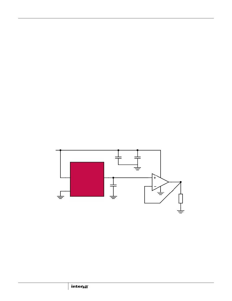
�10μF�
�VIN�
�VOUT�
�VOUT�
�SENSE�
�0.1μF� -� 10μF�
�GND�
�LOAD�
�FIGURE� 53.� KELVIN� SENSED� LOAD�
�18�
�FN7896.1�
�December� 8,� 2011�
�相关PDF资料 |
PDF描述 |
|---|---|
| 1499690-4 | AMPTRAC I/O 2MM CABLE 2POS 4FT |
| 1025R-30K | COIL 2.7UH MOLDED UNSHIELDED |
| ISL21010CFH341Z-TK | IC INTERFACE |
| VI-JTT-EY | CONVERTER MOD DC/DC 6.5V 50W |
| ISL21010CFH325Z-TK | IC INTERFACE |
相关代理商/技术参数 |
参数描述 |
|---|---|
| ISL2101A | 制造商:INTERSIL 制造商全称:Intersil Corporation 功能描述:100V, 2A Peak, High Frequency Half-Bridge Drivers |
| ISL2101AABZ | 功能描述:功率驱动器IC 100V/2A H-BRDG DRVR 8LD RoHS:否 制造商:Micrel 产品:MOSFET Gate Drivers 类型:Low Cost High or Low Side MOSFET Driver 上升时间: 下降时间: 电源电压-最大:30 V 电源电压-最小:2.75 V 电源电流: 最大功率耗散: 最大工作温度:+ 85 C 安装风格:SMD/SMT 封装 / 箱体:SOIC-8 封装:Tube |
| ISL2101AABZ-T | 功能描述:功率驱动器IC 100V/2A H-BRDG DRVR 8LD RoHS:否 制造商:Micrel 产品:MOSFET Gate Drivers 类型:Low Cost High or Low Side MOSFET Driver 上升时间: 下降时间: 电源电压-最大:30 V 电源电压-最小:2.75 V 电源电流: 最大功率耗散: 最大工作温度:+ 85 C 安装风格:SMD/SMT 封装 / 箱体:SOIC-8 封装:Tube |
| ISL2101AAR3Z | 功能描述:功率驱动器IC 100V/2A H-BRDG DRVR 9LD 3X3 TTL INPUTS RoHS:否 制造商:Micrel 产品:MOSFET Gate Drivers 类型:Low Cost High or Low Side MOSFET Driver 上升时间: 下降时间: 电源电压-最大:30 V 电源电压-最小:2.75 V 电源电流: 最大功率耗散: 最大工作温度:+ 85 C 安装风格:SMD/SMT 封装 / 箱体:SOIC-8 封装:Tube |
| ISL2101AAR3Z-T | 功能描述:功率驱动器IC 100V/2A H-BRDG DRVR 9LD 3X3 TTL INPUTS RoHS:否 制造商:Micrel 产品:MOSFET Gate Drivers 类型:Low Cost High or Low Side MOSFET Driver 上升时间: 下降时间: 电源电压-最大:30 V 电源电压-最小:2.75 V 电源电流: 最大功率耗散: 最大工作温度:+ 85 C 安装风格:SMD/SMT 封装 / 箱体:SOIC-8 封装:Tube |
发布紧急采购,3分钟左右您将得到回复。