- 您现在的位置:买卖IC网 > PDF目录16753 > ISL21032DPH306Z-TK (Intersil)IC VREF SERIES PREC 0.6V SOT23-3 PDF资料下载
参数资料
| 型号: | ISL21032DPH306Z-TK |
| 厂商: | Intersil |
| 文件页数: | 5/7页 |
| 文件大小: | 0K |
| 描述: | IC VREF SERIES PREC 0.6V SOT23-3 |
| 标准包装: | 1,000 |
| 系列: | FGA™ |
| 基准类型: | 串联,精度 |
| 输出电压: | 0.6V |
| 容差: | ±6mV |
| 输入电压: | 2.7 V ~ 5.5 V |
| 通道数: | 1 |
| 电流 - 静态: | 25µA |
| 电流 - 输出: | 7mA |
| 工作温度: | -40°C ~ 130°C |
| 安装类型: | 表面贴装 |
| 封装/外壳: | TO-236-3,SC-59,SOT-23-3 |
| 供应商设备封装: | SOT-23-3 |
| 包装: | 带卷 (TR) |
�� �
�
�ISL21032�
�Typical� Performance� Curves,� ISL21032� Low� Voltage� Output� Reference�
�V� IN� =� 3.0V,� I� OUT� =� 0mA,� T� A� =� +25°C� Unless� Otherwise� Specified� (Continued)�
�120�
�100�
�NO� LOAD�
�1nF� LOAD�
�10nF� LOAD�
�80�
�100nF� LOAD�
�60�
�40�
�20�
�0�
�1�
�10�
�100� 1k� 10k�
�100k�
�1M�
�FREQUENCY� (Hz)�
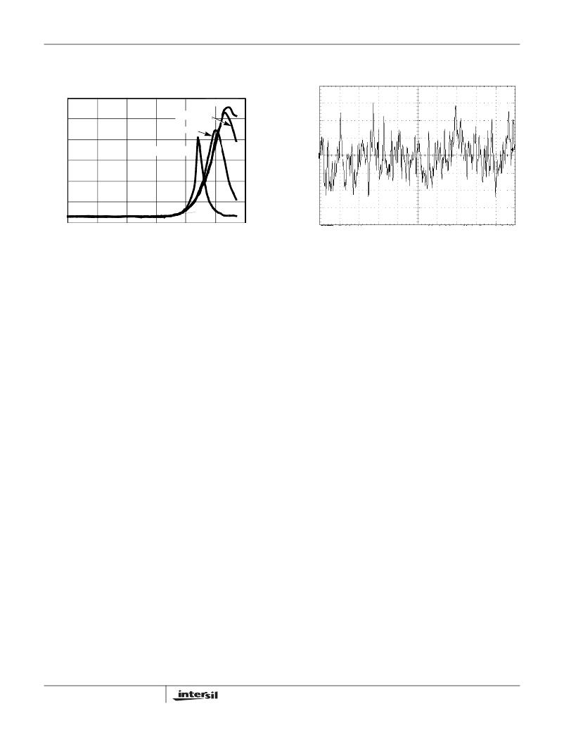
�FIGURE� 13.� Z� OUT� vs� f� vs� C� L�
�FGA� Technology�
�The� ISL21032� series� of� voltage� references� use� the� floating�
�gate� technology� to� create� references� with� very� low� drift� and�
�supply� current.� Essentially� the� charge� stored� on� a� floating�
�gate� cell� is� set� precisely� in� manufacturing.� The� reference�
�voltage� output� itself� is� a� buffered� version� of� the� floating� gate�
�voltage.� The� resulting� reference� device� has� excellent�
�characteristics� which� are� unique� in� the� industry:� very� low�
�temperature� drift,� high� initial� accuracy,� and� almost� zero�
�supply� current.� Also,� the� reference� voltage� itself� is� not� limited�
�by� voltage� bandgaps� or� zener� settings,� so� a� wide� range� of�
�reference� voltages� can� be� programmed� (standard� voltage�
�settings� are� provided,� but� customer-specific� voltages� are�
�available).�
�The� process� used� for� these� reference� devices� is� a� floating�
�gate� CMOS� process,� and� the� amplifier� circuitry� uses� CMOS�
�transistors� for� amplifier� and� output� transistor� circuitry.� While�
�providing� excellent� accuracy,� there� are� limitations� in� output�
�noise� level� and� load� regulation� due� to� the� MOS� device�
�characteristics.� These� limitations� are� addressed� with� circuit�
�techniques� discussed� in� other� sections.�
�Board� Mounting� Considerations�
�For� applications� requiring� the� highest� accuracy,� board�
�mounting� location� should� be� reviewed.� Placing� the� device� in�
�areas� subject� to� slight� twisting� can� cause� degradation� of� the�
�accuracy� of� the� reference� voltage� due� to� die� stresses.� It� is�
�normally� best� to� place� the� device� near� the� edge� of� a� board,�
�or� the� shortest� side,� as� the� axis� of� bending� is� most� limited� at�
�that� location.� Obviously� mounting� the� device� on� flexprint� or�
�extremely� thin� PC� material� will� likewise� cause� loss� of�
�reference� accuracy.�
�5�
�10s/DIV�
�FIGURE� 14.� V� OUT� NOISE�
�Board� Assembly� Considerations�
�FGA� references� provide� high� accuracy� and� low� temperature�
�drift� but� some� PC� board� assembly� precautions� are�
�necessary.� Normal� Output� voltage� shifts� of� 100μV� to� 1mV�
�can� be� expected� with� Pb-free� reflow� profiles� or� wave� solder�
�on� multi-layer� FR4� PC� boards.� Precautions� should� be� taken�
�to� avoid� excessive� heat� or� extended� exposure� to� high� reflow�
�or� wave� solder� temperatures,� this� may� reduce� device� initial�
�accuracy.�
�Post-assembly� x-ray� inspection� may� also� lead� to� permanent�
�changes� in� device� output� voltage� and� should� be� minimized�
�or� avoided.� If� x-ray� inspection� is� required,� it� is� advisable� to�
�monitor� the� reference� output� voltage� to� verify� excessive� shift�
�has� not� occurred.� If� large� amounts� of� shift� are� observed,� it� is�
�best� to� add� an� X-ray� shield� consisting� of� thin� zinc� (300μm)�
�sheeting� to� allow� clear� imaging,� yet� block� x-ray� energy� that�
�affects� the� FGA� reference.�
�Special� Applications� Considerations�
�In� addition� to� post-assembly� examination,� there� are� also�
�other� X-ray� sources� that� may� affect� the� FGA� reference� long�
�term� accuracy.� Airport� screening� machines� contain� X-rays�
�and� will� have� a� cumulative� effect� on� the� voltage� reference�
�output� accuracy.� Carry-on� luggage� screening� uses� low� level�
�X-rays� and� is� not� a� major� source� of� output� voltage� shift,�
�although� if� a� product� is� expected� to� pass� through� that� type� of�
�screening� over� 100� times� it� may� need� to� consider� shielding�
�with� copper� or� aluminum.� Checked� luggage� X-rays� are�
�higher� intensity� and� can� cause� output� voltage� shift� in� much�
�fewer� passes,� so� devices� expected� to� go� through� those�
�machines� should� definitely� consider� shielding.� Note� that� just�
�two� layers� of� 1/2� ounce� copper� planes� will� reduce� the�
�received� dose� by� over� 90%.� The� leadframe� for� the� device�
�which� is� on� the� bottom� also� provides� similar� shielding.�
�FN6239.2�
�September� 28,� 2009�
�相关PDF资料 |
PDF描述 |
|---|---|
| H3CCS-2018M | IDC CABLE - HKC20S/AE20M/HKC20S |
| 301A048-4/86-0 | BOOT MOLDED |
| 202D185-12-0 | BOOT MOLDED |
| 301A048-25-0 | BOOT MOLDED |
| 301A048-4-0 | BOOT MOLDED |
相关代理商/技术参数 |
参数描述 |
|---|---|
| ISL21032-EVALZ | 功能描述:电源管理IC开发工具 ISL21032-EVALZ EVAL BRD ROHS COMPLAINT RoHS:否 制造商:Maxim Integrated 产品:Evaluation Kits 类型:Battery Management 工具用于评估:MAX17710GB 输入电压: 输出电压:1.8 V |
| ISL21060 | 制造商:INTERSIL 制造商全称:Intersil Corporation 功能描述:Precision, Low Noise FGA Voltage References |
| ISL21060BFH620Z-TK | 功能描述:基准电压& 基准电流 048VFERENCE I/A=+/-1 0MV T/C=10PPM RoHS:否 制造商:STMicroelectronics 产品:Voltage References 拓扑结构:Shunt References 参考类型:Programmable 输出电压:1.24 V to 18 V 初始准确度:0.25 % 平均温度系数(典型值):100 PPM / C 串联 VREF - 输入电压(最大值): 串联 VREF - 输入电压(最小值): 分流电流(最大值):60 mA 最大工作温度:+ 125 C 封装 / 箱体:SOT-23-3L 封装:Reel |
| ISL21060BFH625Z-TK | 功能描述:基准电压& 基准电流 PBFREE 2 5VFERENCE I/A=+/-1 0MV RoHS:否 制造商:STMicroelectronics 产品:Voltage References 拓扑结构:Shunt References 参考类型:Programmable 输出电压:1.24 V to 18 V 初始准确度:0.25 % 平均温度系数(典型值):100 PPM / C 串联 VREF - 输入电压(最大值): 串联 VREF - 输入电压(最小值): 分流电流(最大值):60 mA 最大工作温度:+ 125 C 封装 / 箱体:SOT-23-3L 封装:Reel |
| ISL21060BFH630Z-TK | 功能描述:基准电压& 基准电流 PBFREE 3 0VFERENCE I/A=+/-1 0MV RoHS:否 制造商:STMicroelectronics 产品:Voltage References 拓扑结构:Shunt References 参考类型:Programmable 输出电压:1.24 V to 18 V 初始准确度:0.25 % 平均温度系数(典型值):100 PPM / C 串联 VREF - 输入电压(最大值): 串联 VREF - 输入电压(最小值): 分流电流(最大值):60 mA 最大工作温度:+ 125 C 封装 / 箱体:SOT-23-3L 封装:Reel |
发布紧急采购,3分钟左右您将得到回复。