参数资料
| 型号: | ISL23318UFUZ |
| 厂商: | Intersil |
| 文件页数: | 5/19页 |
| 文件大小: | 0K |
| 描述: | IC DGTL POT 1CH 50K 10MSOP |
| 标准包装: | 1,000 |
| 系列: | XDCP™ |
| 接片: | 128 |
| 电阻(欧姆): | 50k |
| 电路数: | 1 |
| 温度系数: | 标准值 85 ppm/°C |
| 存储器类型: | 易失 |
| 接口: | I²C(设备位址) |
| 电源电压: | 1.2 V ~ 5.5 V,1.7 V ~ 5.5 V |
| 工作温度: | -40°C ~ 125°C |
| 安装类型: | 表面贴装 |
| 封装/外壳: | 10-TFSOP,10-MSOP(0.118",3.00mm 宽) |
| 供应商设备封装: | 10-MSOP |
| 包装: | 管件 |
ISL23318
13
FN7887.0
July 26, 2011
Functional Pin Descriptions
Potentiometers Pins
RH AND RL
The high (RH) and low (RL) terminals of the ISL23318 are
equivalent to the fixed terminals of a mechanical potentiometer.
RH and RL are referenced to the relative position of the wiper and
not the voltage potential on the terminals. With WR set to 127
decimal, the wiper will be closest to RH, and with the WR set to 0,
the wiper is closest to RL.
RW
RW is the wiper terminal, and it is equivalent to the movable
terminal of a mechanical potentiometer. The position of the
wiper within the array is determined by the WR register.
Bus Interface Pins
SERIAL DATA INPUT/OUTPUT (SDA)
The SDA is a bidirectional serial data input/output pin for I2C
interface. It receives device address, wiper address and data
from an I2C external master device at the rising edge of the serial
clock SCL, and it shifts out data after each falling edge of the
serial clock.
SDA requires an external pull-up resistor, since it is an open drain
input/output.
SERIAL CLOCK (SCL)
This input is the serial clock of the I2C serial interface. SCL
requires an external pull-up resistor, since a master is an open
drain output.
DEVICE ADDRESS (A1, A0)
The address inputs are used to set the least significant 2 bits of
the 7-bit I2C interface slave address. A match in the slave
address serial data stream must match with the Address input
pins in order to initiate communication with the ISL23318. A
maximum of four ISL23318 devices may occupy the I2C serial
bus (see Table 3).
VLOGIC
This is an input pin that supplies internal level translator for serial
bus operation from 1.2V to 5.5V.
Principles of Operation
The ISL23318 is an integrated circuit incorporating one DCP with
its associated registers and an I2C serial interface providing
direct communication between a host and the potentiometer.
The resistor array is comprised of individual resistors connected
in series. At either end of the array and between each resistor is
an electronic switch that transfers the potential at that point to
the wiper.
The electronic switches on the device operate in a
“make-before-break” mode when the wiper changes tap
positions.
Voltage at any DCP pins, RH, RL or RW, should not exceed VCC
level at any conditions during power-up and normal operation.
The VLOGIC pin needs to be connected to the I2C bus supply
which allows reliable communication with the wide range of
microcontrollers and independent of the VCC level. This is
extremely important in systems where the master supply has
lower levels than DCP analog supply.
DCP Description
The DCP is implemented with a combination of resistor
elements and CMOS switches. The physical ends of each DCP
are equivalent to the fixed terminals of a mechanical
potentiometer (RH and RL pins). The RW pin of the DCP is
connected to intermediate nodes, and is equivalent to the wiper
terminal of a mechanical potentiometer. The position of the
wiper terminal within the DCP is controlled by a 7-bit volatile
Wiper Register (WR). When the WR of a DCP contains all zeroes
(WR[7:0] = 00h), its wiper terminal (RW) is closest to its “Low”
terminal (RL). When the WR register of a DCP contains all ones
(WR[7:0] = 7Fh), its wiper terminal (RW) is closest to its “High”
terminal (RH). As the value of the WR increases from all zeroes
(0) to 0111 1111b (127 decimal), the wiper moves
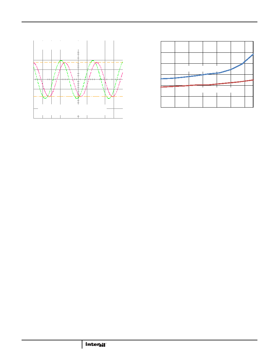
FIGURE 23. 10k -3dB CUT OFF FREQUENCY
FIGURE 24. STANDBY CURRENT vs TEMPERATURE
Typical Performance Curves (Continued)
RTOTAL = 10k
-3dB FREQUENCY = 1.4MHz AT MIDDLE TAP
CH1: 0.5V/DIV, 0.2s/DIV RH PIN
CH2: 0.2V/DIV, 0.2s/DIV RW PIN
0
0.2
0.4
0.6
0.8
1.0
1.2
-40
-15
10
35
60
85
110
S
T
A
N
D
B
Y
C
U
R
E
N
T
I C
C
(
A
)
TEMPERATURE (°C)
VCC = 5.5V, VLOGIC = 5.5V
VCC = 1.7V, VLOGIC = 1.2V
相关PDF资料 |
PDF描述 |
|---|---|
| ISL23418UFRUZ-TK | IC DGTL POT 1CH 50K 10UTQFN |
| VE-25Z-MV-B1 | CONVERTER MOD DC/DC 2V 60W |
| DS1135LZ-12+T&R | IC DELAY LINE 12NS 8-SOIC |
| DS1135LZ-30+T&R | IC DELAY LINE 30NS 8-SOIC |
| VE-2TF-MX-B1 | CONVERTER MOD DC/DC 72V 75W |
相关代理商/技术参数 |
参数描述 |
|---|---|
| ISL23318UFUZ-T7A | 功能描述:数字电位计 IC 128 TAPVOLATILE I2C SNG RNG IND DCP 10LD RoHS:否 制造商:Maxim Integrated 电阻:200 Ohms 温度系数:35 PPM / C 容差:25 % POT 数量:Dual 每 POT 分接头:256 弧刷存储器:Volatile 缓冲刷: 数字接口:Serial (3-Wire, SPI) 描述/功能:Dual Volatile Low Voltage Linear Taper Digital Potentiometer 工作电源电压:1.7 V to 5.5 V 电源电流:27 uA 最大工作温度:+ 125 C 安装风格:SMD/SMT 封装 / 箱体:TQFN-16 封装:Reel |
| ISL23318UFUZ-TK | 功能描述:数字电位计 IC 128 TAP VOLATILE I2C SINGLE FL DCP 10LD RoHS:否 制造商:Maxim Integrated 电阻:200 Ohms 温度系数:35 PPM / C 容差:25 % POT 数量:Dual 每 POT 分接头:256 弧刷存储器:Volatile 缓冲刷: 数字接口:Serial (3-Wire, SPI) 描述/功能:Dual Volatile Low Voltage Linear Taper Digital Potentiometer 工作电源电压:1.7 V to 5.5 V 电源电流:27 uA 最大工作温度:+ 125 C 安装风格:SMD/SMT 封装 / 箱体:TQFN-16 封装:Reel |
| ISL23318WFRUZ-T7A | 功能描述:数字电位计 IC 128 TAPVOLATILE I2C SNG RNG IND DCP 10LD RoHS:否 制造商:Maxim Integrated 电阻:200 Ohms 温度系数:35 PPM / C 容差:25 % POT 数量:Dual 每 POT 分接头:256 弧刷存储器:Volatile 缓冲刷: 数字接口:Serial (3-Wire, SPI) 描述/功能:Dual Volatile Low Voltage Linear Taper Digital Potentiometer 工作电源电压:1.7 V to 5.5 V 电源电流:27 uA 最大工作温度:+ 125 C 安装风格:SMD/SMT 封装 / 箱体:TQFN-16 封装:Reel |
| ISL23318WFRUZ-TK | 功能描述:数字电位计 IC 128 TAP VOLATILE I2C SINGLE FL DCP 10LD RoHS:否 制造商:Maxim Integrated 电阻:200 Ohms 温度系数:35 PPM / C 容差:25 % POT 数量:Dual 每 POT 分接头:256 弧刷存储器:Volatile 缓冲刷: 数字接口:Serial (3-Wire, SPI) 描述/功能:Dual Volatile Low Voltage Linear Taper Digital Potentiometer 工作电源电压:1.7 V to 5.5 V 电源电流:27 uA 最大工作温度:+ 125 C 安装风格:SMD/SMT 封装 / 箱体:TQFN-16 封装:Reel |
| ISL23318WFUZ | 功能描述:数字电位计 IC 128 TAP VOLATILE I2C SINGLE FL DCP 10LD RoHS:否 制造商:Maxim Integrated 电阻:200 Ohms 温度系数:35 PPM / C 容差:25 % POT 数量:Dual 每 POT 分接头:256 弧刷存储器:Volatile 缓冲刷: 数字接口:Serial (3-Wire, SPI) 描述/功能:Dual Volatile Low Voltage Linear Taper Digital Potentiometer 工作电源电压:1.7 V to 5.5 V 电源电流:27 uA 最大工作温度:+ 125 C 安装风格:SMD/SMT 封装 / 箱体:TQFN-16 封装:Reel |
发布紧急采购,3分钟左右您将得到回复。