参数资料
| 型号: | ISL23325WFRUZ-T7A |
| 厂商: | Intersil |
| 文件页数: | 8/20页 |
| 文件大小: | 0K |
| 描述: | IC DGTL POT DUAL 10K 16UTQFN |
| 标准包装: | 1 |
| 系列: | XDCP™ |
| 接片: | 256 |
| 电阻(欧姆): | 10k |
| 电路数: | 2 |
| 温度系数: | 标准值 125 ppm/°C |
| 存储器类型: | 易失 |
| 接口: | I²C,2 线串口 |
| 电源电压: | 1.2 V ~ 5.5 V,1.7 V ~ 5.5 V |
| 工作温度: | -40°C ~ 125°C |
| 安装类型: | 表面贴装 |
| 封装/外壳: | 16-UFQFN |
| 供应商设备封装: | 16-UTQFN(2.6x1.8) |
| 包装: | 标准包装 |
| 其它名称: | ISL23325WFRUZ-T7ADKR |
ISL23325
16
FN7870.0
June 21, 2011
Write Operation
A Write operation requires a START condition, followed by a valid
Identification Byte, a valid Address Byte, a Data Byte, and a STOP
condition. After each of the three bytes, the ISL23325 responds
with an ACK. The data is transferred from I2C block to the
corresponding register at the 9th clock of the data byte and the
It is possible to perform a sequential Write to all DCP channels
via a single Write operation. The command is initiated by sending
an additional Data Byte after the first Data byte instead of
sending a STOP condition.
Read Operation
A Read operation consists of a three byte instruction followed by
one or more Data Bytes (see Figure 30). The master initiates the
operation issuing the following sequence: a START, the
Identification byte with the R/W bit set to “0”, an Address Byte, a
second START, and a second Identification byte with the R/W bit
set to “1”. After each of the three bytes, the ISL23325 responds
with an ACK; then the ISL23325 transmits Data Byte. The master
terminates the read operation issuing a NACK (ACK) and a STOP
condition following the last bit of the last Data Byte (see
Figure 30).
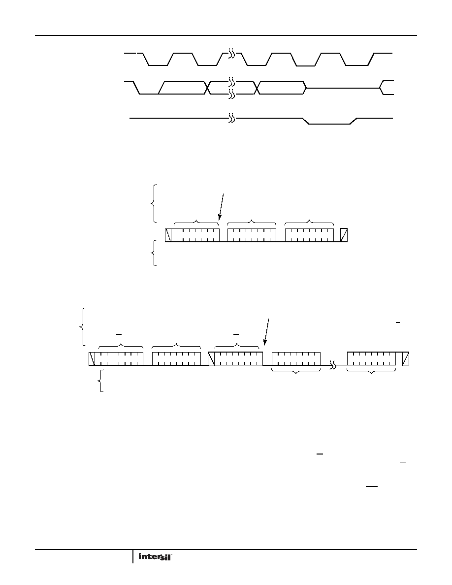
SDA OUTPUT FROM
TRANSMITTER
SDA OUTPUT FROM
RECEIVER
8
1
9
START
ACK
SCL FROM
MASTER
HIGH IMPEDANCE
FIGURE 28. ACKNOWLEDGE RESPONSE FROM RECEIVER
S
T
A
R
T
S
T
O
P
IDENTIFICATION
BYTE
ADDRESS
BYTE
DATA
BYTE
A
C
K
SIGNALS FROM
THE MASTER
SIGNALS FROM
THE SLAVE
A
C
K
10
1
00
A
C
K
WRITE
SIGNAL AT SDA
00 0
A0
A1
FIGURE 29. BYTE WRITE SEQUENCE
A2
SIGNALS
FROM THE
MASTER
SIGNALS FROM
THE SLAVE
SIGNAL AT SDA
S
T
A
R
T
IDENTIFICATION
BYTE WITH
R/W = 0
ADDRESS
BYTE
A
C
K
A
C
K
10
1
00
S
T
O
P
A
C
K
1
IDENTIFICATION
BYTE WITH
R/W = 1
A
C
K
S
T
A
R
T
LAST READ
DATA BYTE
FIRST READ
DATA BYTE
A
C
K
00 0
A0
A1
A0
A1
FIGURE 30. READ SEQUENCE
A
C
K
A2
10 1 0
READ
相关PDF资料 |
PDF描述 |
|---|---|
| D38999/24JE26PC | CONN RCPT 26POS JAM NUT W/PINS |
| MS27468T21A41SB | CONN RCPT 41POS JAM NUT W/SCKT |
| MS27484T24B35P | CONN PLUG 128POS STRAIGHT W/PINS |
| M83723/91W1412N | CONN PLUG 12POS STRAIGHT W/SCKT |
| ISL23325UFRUZ-T7A | IC DGTL POT DUAL 50K 16UTQFN |
相关代理商/技术参数 |
参数描述 |
|---|---|
| ISL23325WFRUZ-TK | 功能描述:数字电位计 IC 256 TAP VOLATILE I2C DL FL RNG DCP 14LD RoHS:否 制造商:Maxim Integrated 电阻:200 Ohms 温度系数:35 PPM / C 容差:25 % POT 数量:Dual 每 POT 分接头:256 弧刷存储器:Volatile 缓冲刷: 数字接口:Serial (3-Wire, SPI) 描述/功能:Dual Volatile Low Voltage Linear Taper Digital Potentiometer 工作电源电压:1.7 V to 5.5 V 电源电流:27 uA 最大工作温度:+ 125 C 安装风格:SMD/SMT 封装 / 箱体:TQFN-16 封装:Reel |
| ISL23325WFVZ | 功能描述:数字电位计 IC 256 TAP VOLATILE I2C DL FL RNG DCP 14LD RoHS:否 制造商:Maxim Integrated 电阻:200 Ohms 温度系数:35 PPM / C 容差:25 % POT 数量:Dual 每 POT 分接头:256 弧刷存储器:Volatile 缓冲刷: 数字接口:Serial (3-Wire, SPI) 描述/功能:Dual Volatile Low Voltage Linear Taper Digital Potentiometer 工作电源电压:1.7 V to 5.5 V 电源电流:27 uA 最大工作温度:+ 125 C 安装风格:SMD/SMT 封装 / 箱体:TQFN-16 封装:Reel |
| ISL23325WFVZ-T7A | 功能描述:数字电位计 IC 256 TAPVOLATILE I2C DUAL FL RNG IND 14LD RoHS:否 制造商:Maxim Integrated 电阻:200 Ohms 温度系数:35 PPM / C 容差:25 % POT 数量:Dual 每 POT 分接头:256 弧刷存储器:Volatile 缓冲刷: 数字接口:Serial (3-Wire, SPI) 描述/功能:Dual Volatile Low Voltage Linear Taper Digital Potentiometer 工作电源电压:1.7 V to 5.5 V 电源电流:27 uA 最大工作温度:+ 125 C 安装风格:SMD/SMT 封装 / 箱体:TQFN-16 封装:Reel |
| ISL23325WFVZ-TK | 功能描述:数字电位计 IC 256 TAP VOLATILE I2C DL FL RNG DCP 14LD RoHS:否 制造商:Maxim Integrated 电阻:200 Ohms 温度系数:35 PPM / C 容差:25 % POT 数量:Dual 每 POT 分接头:256 弧刷存储器:Volatile 缓冲刷: 数字接口:Serial (3-Wire, SPI) 描述/功能:Dual Volatile Low Voltage Linear Taper Digital Potentiometer 工作电源电压:1.7 V to 5.5 V 电源电流:27 uA 最大工作温度:+ 125 C 安装风格:SMD/SMT 封装 / 箱体:TQFN-16 封装:Reel |
| ISL23328 | 制造商:INTERSIL 制造商全称:Intersil Corporation 功能描述:Dual, 128-Tap, Low Voltage Digitally Controlled Potentiometer (XDCPa?¢) |
发布紧急采购,3分钟左右您将得到回复。