参数资料
| 型号: | ISL23415TFRUZ-TK |
| 厂商: | Intersil |
| 文件页数: | 5/20页 |
| 文件大小: | 0K |
| 描述: | IC DGTL POT 256POS 100K 10TQFN |
| 产品培训模块: | Solutions for Industrial Control Applications |
| 标准包装: | 1,000 |
| 系列: | XDCP™ |
| 接片: | 256 |
| 电阻(欧姆): | 100k |
| 电路数: | 1 |
| 温度系数: | 标准值 70 ppm/°C |
| 存储器类型: | 易失 |
| 接口: | 4 线 SPI(芯片选择) |
| 电源电压: | 1.2 V ~ 5.5 V,1.7 V ~ 5.5 V |
| 工作温度: | -40°C ~ 125°C |
| 安装类型: | 表面贴装 |
| 封装/外壳: | 10-UFQFN |
| 供应商设备封装: | 10-UTQFN(2.1x1.6) |
| 包装: | 带卷 (TR) |
ISL23415
13
FN7780.1
August 16, 2011
Functional Pin Description
Potentiometers Pins
RH AND RL
The high (RH) and low (RL) terminals of the ISL23415 are
equivalent to the fixed terminals of a mechanical potentiometer.
The RH and RL are referenced to the relative position of the wiper
and not the voltage potential on the terminals. With the WR
register set to 255 decimal, the wiper will be closest to RH, and
with the WR register set to 0, the wiper is closest to RL.
RW
The RW is the wiper terminal, and it is equivalent to the
moveable terminal of a mechanical potentiometer. The position
of the wiper within the array is determined by the WR register.
Power Pins
VCC
Power terminal for the potentiometer section analog power
source. Can be any value needed to support voltage range of DCP
pins, from 1.7V to 5.5V, independent of the VLOGIC voltage.
Bus Interface Pins
SERIAL CLOCK (SCL)
This input is the serial clock of the SPI serial interface.
SERIAL DATA INPUT (SDI)
The SDI is a serial data input pin for SPI interface. It receives
operation code, wiper address and data from the SPI remote
host device. The data bits are shifted in at the rising edge of the
serial clock SCK, while the CS input is low.
SERIAL DATA OUTPUT (SDO)
The SDO is a serial data output pin. During a read cycle, the data
bits are shifted out on the falling edge of the serial clock SCK and
will be available to the master on the following rising edge of SCK.
The output type is configured through ACR[1] bit for Push-Pull or
Open Drain operation. Default setting for this pin is Push-Pull. An
external pull-up resistor is required for Open Drain output
operation. When CS is HIGH, the SDO pin is in tri-state (Z) or
high-tri-state (Hi-Z) depends on the selected configuration.
CHIP SELECT (CS)
CS LOW enables the ISL23415, placing it in the active power
mode. A HIGH to LOW transition on CS is required prior to the
start of any operation after power-up. When CS is HIGH, the
ISL23415 is deselected and the SDO pin is at high impedance,
and the device will be in the standby state.
VLOGIC
Digital power source for the logic control section. It supplies an
internal level translator for 1.2V to 5.5V serial bus operation. Use
the same supply as the I2C logic source.
Principles of Operation
The ISL23415 is an integrated circuit incorporating one DCP with
its associated registers and an SPI serial interface providing
direct communication between a host and the potentiometer.
The resistor array is comprised of individual resistors connected
in series. At either end of the array and between each resistor is
an electronic switch that transfers the potential at that point to
the wiper.
The electronic switches on the device operate in a “make before
break” mode when the wiper changes tap positions.
Voltage at any DCP pins, RH, RL or RW, should not exceed VCC
level at any conditions during power-up and normal operation.
The VLOGIC pin needs to be connected to the SPI bus supply
which allows reliable communication with the wide range of
microcontrollers and independent of the VCC level. This is
extremely important in systems where the digital supply has
lower levels than the analog supply.
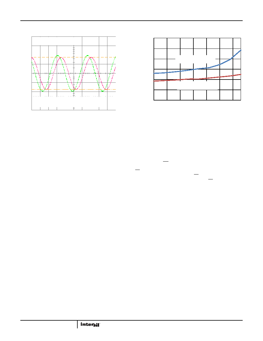
FIGURE 23. 10k -3dB CUT OFF FREQUENCY
FIGURE 24. STANDBY CURRENT vs TEMPERATURE
Typical Performance Curves (Continued)
RTOTAL = 10k
-3dB FREQUENCY = 1.4MHz AT MIDDLE TAP
CH1: 0.5V/DIV, 0.2s/DIV RH PIN
CH2: 0.2V/DIV, 0.2s/DIV RW PIN
0
0.2
0.4
0.6
0.8
1.0
1.2
-40
-15
10
35
60
85
110
S
T
A
N
D
B
Y
C
U
R
E
N
T
I C
C
(
A
)
TEMPERATURE (°C)
VCC = 5.5V, VLOGIC = 5.5V
VCC = 1.7V, VLOGIC = 1.2V
相关PDF资料 |
PDF描述 |
|---|---|
| VE-B5B-MY-F2 | CONVERTER MOD DC/DC 95V 50W |
| DS1135LU-30 | IC DELAY LINE 30NS 8-USOP |
| ISL23315WFRUZ-TK | IC DGTL POT 256POS 10K 10TQFN |
| DS1135LU-20+ | IC DELAY LINE 20NS 8-USOP |
| VE-B5B-MY-F1 | CONVERTER MOD DC/DC 95V 50W |
相关代理商/技术参数 |
参数描述 |
|---|---|
| ISL23415TFUZ | 功能描述:数字电位计 IC 256 TAP VOLATILE SPI DL FL RNG DCP 10LD RoHS:否 制造商:Maxim Integrated 电阻:200 Ohms 温度系数:35 PPM / C 容差:25 % POT 数量:Dual 每 POT 分接头:256 弧刷存储器:Volatile 缓冲刷: 数字接口:Serial (3-Wire, SPI) 描述/功能:Dual Volatile Low Voltage Linear Taper Digital Potentiometer 工作电源电压:1.7 V to 5.5 V 电源电流:27 uA 最大工作温度:+ 125 C 安装风格:SMD/SMT 封装 / 箱体:TQFN-16 封装:Reel |
| ISL23415TFUZ-T7A | 功能描述:数字电位计 IC 256 TAP VOLATILE SPI DL FL RNG DCP 10LD RoHS:否 制造商:Maxim Integrated 电阻:200 Ohms 温度系数:35 PPM / C 容差:25 % POT 数量:Dual 每 POT 分接头:256 弧刷存储器:Volatile 缓冲刷: 数字接口:Serial (3-Wire, SPI) 描述/功能:Dual Volatile Low Voltage Linear Taper Digital Potentiometer 工作电源电压:1.7 V to 5.5 V 电源电流:27 uA 最大工作温度:+ 125 C 安装风格:SMD/SMT 封装 / 箱体:TQFN-16 封装:Reel |
| ISL23415TFUZ-TK | 功能描述:数字电位计 IC 256 TAP VOLATILE SPI DL FL RNG DCP 10LD RoHS:否 制造商:Maxim Integrated 电阻:200 Ohms 温度系数:35 PPM / C 容差:25 % POT 数量:Dual 每 POT 分接头:256 弧刷存储器:Volatile 缓冲刷: 数字接口:Serial (3-Wire, SPI) 描述/功能:Dual Volatile Low Voltage Linear Taper Digital Potentiometer 工作电源电压:1.7 V to 5.5 V 电源电流:27 uA 最大工作温度:+ 125 C 安装风格:SMD/SMT 封装 / 箱体:TQFN-16 封装:Reel |
| ISL23415UFRUZ-T7A | 功能描述:数字电位计 IC 256 TAP VOLATILE SPI FL RNG INC DCP 21X16 RoHS:否 制造商:Maxim Integrated 电阻:200 Ohms 温度系数:35 PPM / C 容差:25 % POT 数量:Dual 每 POT 分接头:256 弧刷存储器:Volatile 缓冲刷: 数字接口:Serial (3-Wire, SPI) 描述/功能:Dual Volatile Low Voltage Linear Taper Digital Potentiometer 工作电源电压:1.7 V to 5.5 V 电源电流:27 uA 最大工作温度:+ 125 C 安装风格:SMD/SMT 封装 / 箱体:TQFN-16 封装:Reel |
| ISL23415UFRUZ-TK | 功能描述:数字电位计 IC 256 TAP VOLATILE SPI FL RNG INC DCP 21X16 RoHS:否 制造商:Maxim Integrated 电阻:200 Ohms 温度系数:35 PPM / C 容差:25 % POT 数量:Dual 每 POT 分接头:256 弧刷存储器:Volatile 缓冲刷: 数字接口:Serial (3-Wire, SPI) 描述/功能:Dual Volatile Low Voltage Linear Taper Digital Potentiometer 工作电源电压:1.7 V to 5.5 V 电源电流:27 uA 最大工作温度:+ 125 C 安装风格:SMD/SMT 封装 / 箱体:TQFN-16 封装:Reel |
发布紧急采购,3分钟左右您将得到回复。