- 您现在的位置:买卖IC网 > PDF目录383129 > ISL24006IR-T7 (INTERSIL CORP) MINIATURE TOGGLE SWITCH PDF资料下载
参数资料
| 型号: | ISL24006IR-T7 |
| 厂商: | INTERSIL CORP |
| 元件分类: | 模拟信号调理 |
| 英文描述: | MINIATURE TOGGLE SWITCH |
| 中文描述: | SPECIALTY ANALOG CIRCUIT, QCC38 |
| 封装: | MO-220, QFN-38 |
| 文件页数: | 7/10页 |
| 文件大小: | 435K |
| 代理商: | ISL24006IR-T7 |
7
FN6110.1
September 9, 2005
For the Standard mode in a READ transfer, a master device
accepts data from the ISL24006. The output data byte
(DATA 1) of the first channel (OUT1) is the second byte of
the transfer. OUT2 output data byte is the third byte of the
transfer, and so forth and so on. The ISL24006 sends an
acknowledge bit after every eighth bit to tell the master
device that the ISL24006 is ready to send another byte.
Consequently, the master must send a Not Acknowledge,
(NA) at the end of the 14th data byte to tell ISL24006 to
release the SDA bus.
See Timing Diagram 1 (Figure 1) for detailed formats.
Devices Address and W/R Bit
Data transfers follow the format shown in Timing Diagram 1.
After the Start condition, a first byte is sent which contains
the Device Address and write/read bit. This address is a 7-bit
long device address and only two device addresses hex (74)
and hex (75) in binary, bin (111010) and bin (111011) are
allowed for the ISL24006. The first 6 bits (A6 to A1, MSBs) of
the device address have been factory programmed and are
always 111010. Only the least significant bit (LSB) A0 is
allowed to change the logic state. This LSB is controlled
externally on the pin #4, A0. When pulled high to D
VDD
, the
LSB of the device address is high and thus the address is
hex (75) or in binary bin (1110101). When pulled low to GND,
the LSB of the device address low and thus the address is
hex (74) or in binary 1110100. Since the device address has
to be unique in the I
2
C bus line, a maximum of two ISL24006
may be used on the same bus at one time.
The ISL24006 monitors the bus continuously and waiting for
the Start condition followed by the device address. When the
device recognizes its device address, it will start to accept
data. The eighth bit (W/R) following the device address
indicates the data direction. A "0" is a Write transmission; a
master device will send data to the ISL24006 to set or
program a desired reference voltage. A "1" indicates a Read
transmission; the master device will receive data from the
ISL24006 to read the previous data the voltage reference
was set or programmed.
Control Byte
The multi-function control byte contains information that
selects the memory bank (bankA, or bankB), and operation
(output, read, or write). It also controls the OSC pin function
(external or internal).
The second bit, C1, selects which bank to write to. A "
0
"
selects
bankA
. A "
1
" selects
bankB
. C1 is a "don't care" on
a read mode.
The third bit, C2, selects which bank to read from. A "
0
"
selects
bankA
. A "
1
" selects
bankB
. C2 is a "don't care" on
a write mode.
The fourth bit, C3, selects the function of the OSC pin. A "
0
"
selects the internal oscillator. When the internal oscillator is
selected, the OSC pin acts as an output pin. It generates a
square wave with a frequency of typically 20kHz where
multiple chips can be synchronized. A "
1
" selects an external
oscillator. When the external oscillator is selected, the OSC
pin acts an input pin. Multiple chips can be synchronized to
an external oscillator. The external frequency or refresh rate
can be synchronized up to 200kHz typically.
The rest of the bits (C4-C7) in the control byte are "don't
cares".
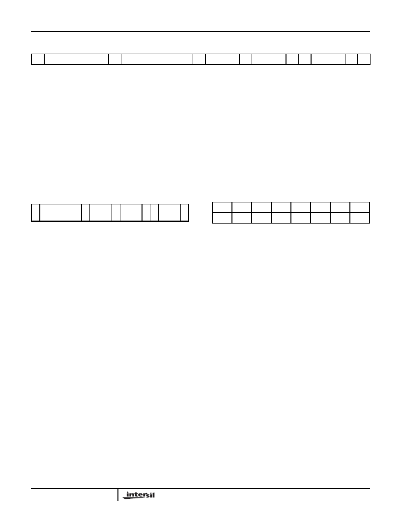
TABLE 1. STANDARD MODE WRITE TRANSFER
S
ISL24006 ADDRESS + W
A
CONTROL BYTE
A
DATA 1
A
DATA 2
A
...
DATA 14
A
P
S = Start condition
CONTROL BYTE = multifunction control
P = Stop condition
DATA 1 = 8-bit input to DAC OUT1
A = Acknowledge bit
DATA 2 = 8-bit input to DAC OUT2
DATA 14 = 8-bit input to DAC OUT14
TABLE 2. Standard Mode READ Transfer
S
ISL24006
ADDRESS + R
A DATA 1 A DATA 2 A ...
DATA
14
P
S = Start condition
A = Acknowledge
P = Stop condition
NA = Not Acknowledge
DATA 1 = 8-bit input to DAC OUT1
DATA 2 = 8-bit input to DAC OUT2
DATA 14 = 8-bit input to DAC OUT14
TABLE 3. Control Byte
C7
C6
C5
C4
C3
C2
C1
C0
X
X
X
X
0
0
0
0
C0
= "0" bypass oscillator
= "1" 3.5μs lagging
C1
= "0" write data to bankA (default)
= "1" write data to bankB
C2
= "0" read data from bankA (default)
= "1" read data from bankB
C3
= "0" internal oscillator (default)
= "1" external oscillator
ISL24006
相关PDF资料 |
PDF描述 |
|---|---|
| ISL24011 | High Voltage TFT-LCD Logic Driver |
| ISL24011IVZ | High Voltage TFT-LCD Logic Driver |
| ISL24011IVZ-T | High Voltage TFT-LCD Logic Driver |
| ISL28136 | 5MHz, Single and Dual Precision Rail-to-Rail Input-Output (RRIO) Op Amps(5MHz,单/双精度轨对轨输入-输出(RRIO)运放) |
| ISL28236 | 5MHz, Single and Dual Precision Rail-to-Rail Input-Output (RRIO) Op Amps(5MHz,单/双精密轨对轨输入-输出(RRIO)运放) |
相关代理商/技术参数 |
参数描述 |
|---|---|
| ISL24006IRZ | 制造商:INTERSIL 制造商全称:Intersil Corporation 功能描述:14-Channel Programmable Switchable I2C TFT-LCD Reference Voltage Generator with Integrated 4-Channel Static Gamma Drivers |
| ISL24006IRZ-T13 | 制造商:Rochester Electronics LLC 功能描述: 制造商:Intersil Corporation 功能描述: |
| ISL24006IRZ-T7 | 制造商:INTERSIL 制造商全称:Intersil Corporation 功能描述:14-Channel Programmable Switchable I2C TFT-LCD Reference Voltage Generator with Integrated 4-Channel Static Gamma Drivers |
| ISL24007IRZ | 制造商:Intersil Corporation 功能描述:PB-FREE 14-CH PROGRAMMABLE SWITCHABLE I2C TFT-LC - Bulk |
| ISL24007IRZ-T13 | 制造商:Intersil Corporation 功能描述:PB-FREE 14-CH PROGRAMMABLE SWITCHABLE I2C TFT-LC - Tape and Reel |
发布紧急采购,3分钟左右您将得到回复。