- 您现在的位置:买卖IC网 > PDF目录383129 > ISL24006IRZ-T7 (INTERSIL CORP) 14-Channel Programmable Switchable I2C TFT-LCD Reference Voltage Generator with Integrated 4-Channel Static Gamma Drivers PDF资料下载
参数资料
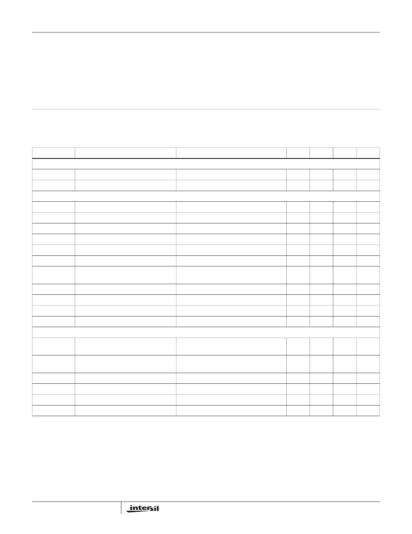
| 型号: | ISL24006IRZ-T7 |
| 厂商: | INTERSIL CORP |
| 元件分类: | 模拟信号调理 |
| 英文描述: | 14-Channel Programmable Switchable I2C TFT-LCD Reference Voltage Generator with Integrated 4-Channel Static Gamma Drivers |
| 中文描述: | SPECIALTY ANALOG CIRCUIT, QCC38 |
| 封装: | ROHS COMPLIANT, MO-220, QFN-38 |
| 文件页数: | 2/10页 |
| 文件大小: | 435K |
| 代理商: | ISL24006IRZ-T7 |
2
FN6110.1
September 9, 2005
IMPORTANT NOTE: All parameters having Min/Max specifications are guaranteed. Typ values are for information purposes only. Unless otherwise noted, all tests are
at the specified temperature and are pulsed tests, therefore: T
J
= T
C
= T
A
Absolute Maximum Ratings
(T
A
= 25°C)
Supply Voltage between A
VDD
and GND . . . . . . . . . . . . . . . . .+18V
Supply Voltage between D
VDD
and GND lesser of V
S
or +7V (max)
Maximum Continuous Output Current . . . . . . . . . . . . 20mA/channel
Operating Temperature . . . . . . . . . . . . . . . . . . . . . . .-40°C to +85°C
Power Dissipation . . . . . . . . . . . . . . . . . . . . . . . . . . . . . . . . . . . TBD
Maximum Die Temperature . . . . . . . . . . . . . . . . . . . . . . . . . .+125°C
Lead Temperature . . . . . . . . . . . . . . . . . . . . . . . . . . . . . . . . .+260°C
Storage Temperature. . . . . . . . . . . . . . . . . . . . . . . .-65°C to +150°C
CAUTION: Stresses above those listed in “Absolute Maximum Ratings” may cause permanent damage to the device. This is a stress only rating and operation of the
device at these or any other conditions above those indicated in the operational sections of this specification is not implied. The device outputs cannot withstand short-
circuit condition for extended periods of time. To avoid damage, do not exceed absolute maximum rating of 20mA/channel.
Electrical Specifications
A
VDD
= 15V, D
VDD
= 5V, V
REFU_H
= 14V, V
REFU_L
= 8.5V, V
REFL_H
= 6.5V, V
REFL_L
= 1V,
R
L
= 1k
and
C
L
= 10pF to 1/2 A
VDD
, T
A
= 25°C, unless otherwise specified.
PARAMETER
DESCRIPTION
CONDITIONS
MIN
TYP
MAX
UNIT
SUPPLY
I
AVDD
Supply Current
No load
30
38
mA
I
DVDD
Digital Supply Current
2.75
4
mA
ANALOG
V
OH
OUT1 to OUT7
V
REFU_H
= 14V, A
VDD
= 15V
13.94
13.98
14.02
V
V
OL
OUT1 to OUT7
V
REFU_L
= 8.5V, A
VDD
= 15V
8.47
8.51
8.55
V
V
OH
OUT8 to OUT14
V
REFL_H
= 6.5V, A
VDD
= 15V
6.44
6.48
6.52
V
V
OL
OUT8 to OUT14
V
REFL_L
= 1.0V, A
VDD
= 15V
0.96
1.00
1.04
V
PSRR
Power Supply Rejection Ratio
A
VDD
is moved from 14V to 16V
42
50
dB
V
AC
Accuracy
-50
0
+50
mV
I
B
Input Bias Current,
V
REF(U_H, U_L, L_H, L_L)
V
REF
= 1/2 A
VDD
2
50
nA
REG
Load Regulation
I
OUT
= 5mA step
0.5
mV/mA
BG
Band Gap
1.1
1.3
1.4
V
SR
Slew Rate
8
15
V/μs
t
S
Settling Time
±1/2 LSB
1
μs
DIGITAL
V
IH
Logic 1 Input Voltage
D
VDD
-
20%
V
V
IL
Logic 0 Input Voltage
20%*
D
VDD
V
F
CLK
Clock Frequency
400
kHz
R
SDIN
S
DIN
Input Resistance
SCL, SDA, STD_REG
1
G
t
S
Setup Time
40
ns
t
H
Hold Time
40
ns
ISL24006
相关PDF资料 |
PDF描述 |
|---|---|
| ISL24006IR-T13 | 14-Channel Programmable Switchable I2C TFT-LCD Reference Voltage Generator with Integrated 4-Channel Static Gamma Drivers |
| ISL24006IR-T7 | MINIATURE TOGGLE SWITCH |
| ISL24011 | High Voltage TFT-LCD Logic Driver |
| ISL24011IVZ | High Voltage TFT-LCD Logic Driver |
| ISL24011IVZ-T | High Voltage TFT-LCD Logic Driver |
相关代理商/技术参数 |
参数描述 |
|---|---|
| ISL24007IRZ | 制造商:Intersil Corporation 功能描述:PB-FREE 14-CH PROGRAMMABLE SWITCHABLE I2C TFT-LC - Bulk |
| ISL24007IRZ-T13 | 制造商:Intersil Corporation 功能描述:PB-FREE 14-CH PROGRAMMABLE SWITCHABLE I2C TFT-LC - Tape and Reel |
| ISL24008IRTZ | 制造商:Intersil Corporation 功能描述: |
| ISL24008IRTZ-T13 | 制造商:Rochester Electronics LLC 功能描述: 制造商:Intersil Corporation 功能描述: |
| ISL24010 | 制造商:INTERSIL 制造商全称:Intersil Corporation 功能描述:High Voltage TFT-LCD Logic Driver |
发布紧急采购,3分钟左右您将得到回复。