参数资料
| 型号: | ISL24010IVZ-T |
| 厂商: | Intersil |
| 文件页数: | 7/9页 |
| 文件大小: | 0K |
| 描述: | IC VOLT SHIFTER TFT/LCD 20-TSSOP |
| 标准包装: | 1 |
| 逻辑功能: | 电平移位器 |
| 位数: | 8 |
| 输入类型: | 电压 |
| 输出类型: | 电压 |
| 通道数: | 1 |
| 输出/通道数目: | 8 |
| 差分 - 输入:输出: | 无/无 |
| 传输延迟(最大): | 150ns |
| 工作温度: | -40°C ~ 85°C |
| 封装/外壳: | 20-TSSOP(0.173",4.40mm 宽) |
| 供应商设备封装: | 20-TSSOP |
| 包装: | 标准包装 |
| 产品目录页面: | 1244 (CN2011-ZH PDF) |
| 其它名称: | ISL24010IVZ-TDKR |
7
Application Information
General
The ISL24010 is an Octal voltage level shifter. The part was
designed to level shifts a digital input signal to +22V and -5V
for TFT-LCD displays. The device is capable of level shifting
a CMOS logic signal between +40V and -20V.
Power Supply Decoupling
The ISL24010 requires a 0.1
F decoupling capacitor as
close to the VON1, VON2 and VOFF power supply pins for a
large load equal to 5k
in parallel with 100pF (Figure 16).
This will deduce any dv/dt between the different supplies and
prevent the internal ESD clamp from turning on and
damaging the part.
Power Supply Sequence
The ISL24010 requires that VON2 be greater than or equal to
VON1 at all times. Therefore, if VON1 and Von 2 are different
supplies, then VON2 needs to be turned on before VON1.
The reason for this requirement is shown in Circuit 4 in the
Pin Description Table. The ESD protection diode between
VON2 and Von 1 will forward bias if VON1 becomes a diode
drop greater than VON2. Recommended power supply
sequence: VON2, VON1, VOFF then input logic signals.
The ESD protection scheme is based on diodes from the
pins to the VON2 supply and a dV/dt- triggered clamp. This
dV/dt triggered clamp imposes a maximum supply turn-on
slew rate of 10V/s. This clamp will trigger if the supply
powers up too fast, causing amps of current to flow. Ground
and VON1 are treated as I/O pins with this protection
scheme. In applications where the dV/dt supply ramp could
exceed 10V/s, such as hot plugging, additional methods
should be employed to ensure the rate of rise is not
exceeded.
Latch-up Proof
The ISL24010 is manufactured in a high voltage DI process
that isolates every transistor in it’s own tub making the part
latch-up proof.
Input Pin Connections
Unused inputs must be tied to ground. Failure to tie unused
input pins to ground will result in a rail to rail oscillations on
the respective output pins and higher unwanted power
dissipation in the part. Under these conditions, the
temperature of the part could get very hot.
Limiting the Output Current
No output short circuit current limit exists on this part. All
applications need to limit the output current to less than
80mA. Adequate thermal heat sinking of the parts is also
required.
Application Diagram (TV)
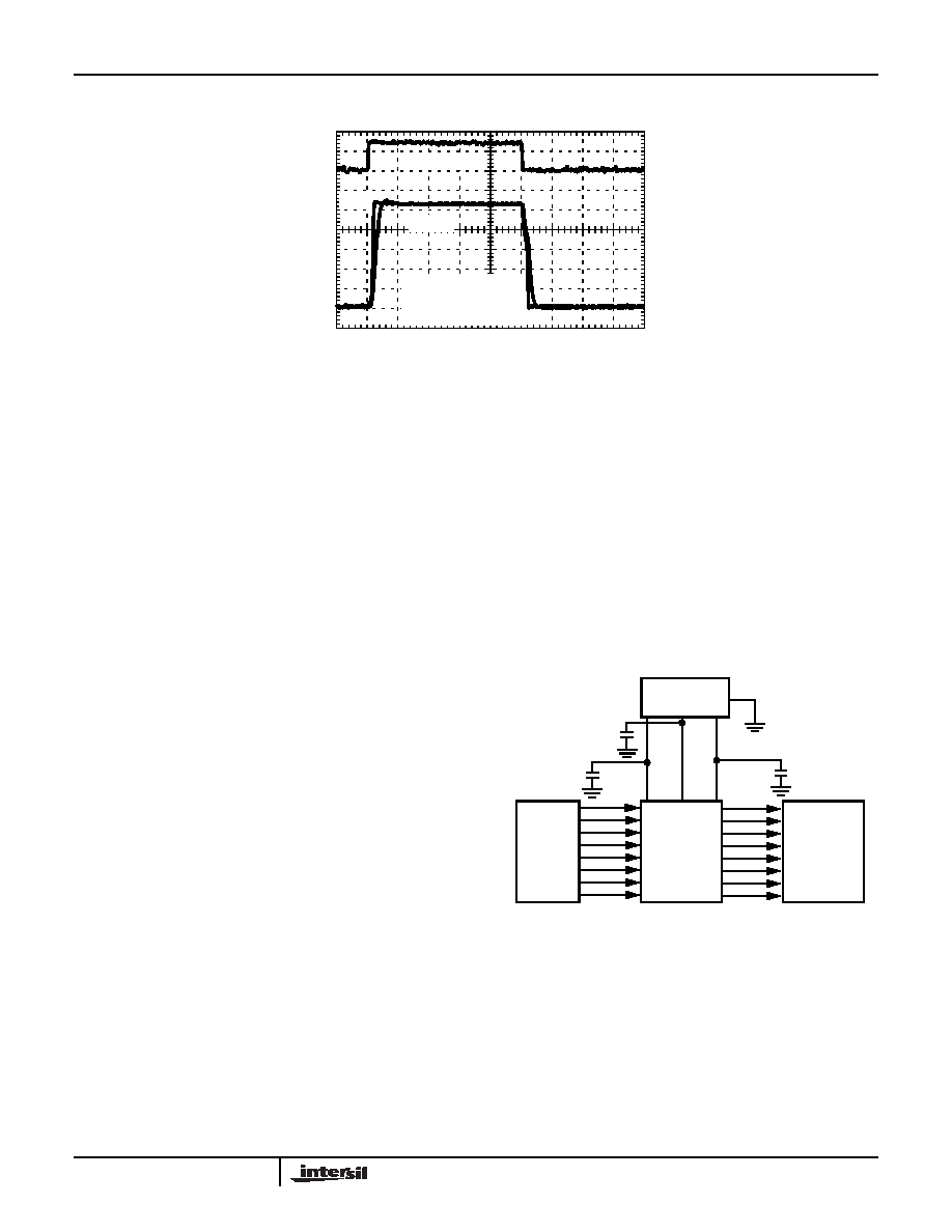
FIGURE 13. TRANSIENT RESPONSE vs LOAD CAPACITANCE
Typical Performance Curves TA = 25°C, Output load parallel RC (RL = 5k, CL = 100pF) unless otherwise specified. (Continued)
0
2s/DIV
VON1 & 2 = 22V
VOFF = -5V
50kHz 50% Duty Cycle
100pF
1500pF
Pulse Input
2V
/D
IV
5V
/DI
V
ISL24010
FIGURE 14. TYPICAL TV APPLICATION CIRCUIT
1.0
F
1.0
F
DC/DC
CONVERTER
TIMING
CON-
LEVEL
LCD PANEL
1.0
F
VON1
VON2
VOFF
SHIFTER
TROLLER
ISL24010
相关PDF资料 |
PDF描述 |
|---|---|
| ISL24201IRTZ | IC VCOM CALIBRATOR I2C 8TDFN |
| ISL24202IRTZ | IC PROG 8BIT VCOM CALIBRTR 8TDFN |
| ISL24211IRTZ | IC VCOM CALIBRATOR I2C 10TDFN |
| ISL24212IRTZ | IC PROG 8BIT VCOM CALIBRTR 10TDF |
| ISL28197FRUZ-T7 | IC COMP RRIO SGL 800NA 6-TDFN |
相关代理商/技术参数 |
参数描述 |
|---|---|
| ISL24011 | 制造商:INTERSIL 制造商全称:Intersil Corporation 功能描述:High Voltage TFT-LCD Logic Driver |
| ISL24011_06 | 制造商:INTERSIL 制造商全称:Intersil Corporation 功能描述:High Voltage TFT-LCD Logic Driver |
| ISL24011IVZ | 功能描述:LCD 驱动器 ISL24011IVZ OCTAL LV LSHIFTER 4700PF LOAD RoHS:否 制造商:Maxim Integrated 数位数量:4.5 片段数量:30 最大时钟频率:19 KHz 工作电源电压:3 V to 3.6 V 最大工作温度:+ 85 C 最小工作温度:- 20 C 封装 / 箱体:PDIP-40 封装:Tube |
| ISL24011IVZ-T | 功能描述:LCD 驱动器 ISL24011IVZ OCTAL LV LSHIFTER 5000PF LOAD RoHS:否 制造商:Maxim Integrated 数位数量:4.5 片段数量:30 最大时钟频率:19 KHz 工作电源电压:3 V to 3.6 V 最大工作温度:+ 85 C 最小工作温度:- 20 C 封装 / 箱体:PDIP-40 封装:Tube |
| ISL24014IRZ | 制造商:Intersil Corporation 功能描述: |
发布紧急采购,3分钟左右您将得到回复。