参数资料
| 型号: | ISL26319FVZ-T7A |
| 厂商: | Intersil |
| 文件页数: | 10/23页 |
| 文件大小: | 0K |
| 描述: | IC ADC 12BIT SRL/SPI 16TSSOP |
| 标准包装: | 1 |
| 位数: | 12 |
| 采样率(每秒): | 125k |
| 数据接口: | 串行,SPI? |
| 转换器数目: | 1 |
| 功率耗散(最大): | 80mW |
| 电压电源: | 单电源 |
| 工作温度: | -40°C ~ 125°C |
| 安装类型: | 表面贴装 |
| 封装/外壳: | 16-TSSOP(0.173",4.40mm 宽) |
| 供应商设备封装: | 16-TSSOP |
| 包装: | 标准包装 |
| 输入数目和类型: | 8 个单端,单极 |
| 其它名称: | ISL26319FVZ-T7ADKR |
ISL26310, ISL26311, ISL26312, ISL26313, ISL26314, ISL26315, ISL26319
18
FN7549.2
February 26, 2014
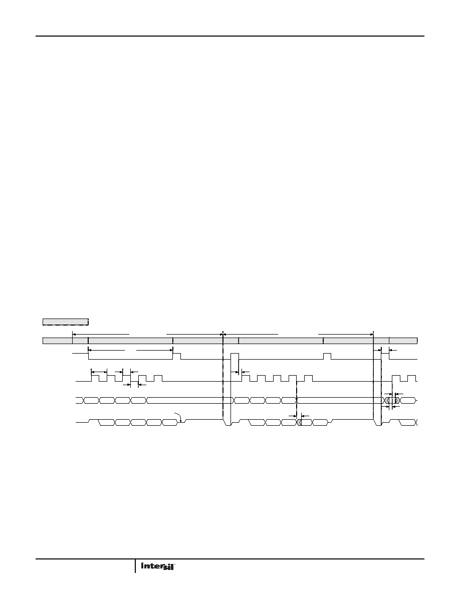
Reading After Conversion Mode, with EOC
In this mode (Figure 33), after CNV is asserted Low to start input
acquisition, a data exchange is executed by SCLK during the
Acquisition period. CNV is asserted High briefly to initiate a
Conversion, forcing SDO to a high-impedance state. SDO returns
HIGH when CNV is asserted Low during the entire conversion period.
At the end of conversion, the device asserts SDO Low to indicate
that the conversion is complete. This may be used as an interrupt
to start the Acquisition phase. It should be noted (as indicated in
Figure 33) that an additional pulse on CNV is required at the end
of conversion to take the part back to Acquisition from Idle state.
As discussed in section “Reading After Conversion Mode Without
throughput at slower SPI clock rates.
Reading During Conversion Mode, with EOC
From Idle, a falling edge on CNV initiates the Acquisition mode,
and then a rising edge initiates a Conversion. After the
conversion is initiated, CNV is asserted Low once again. Data
exchange across SDI and SDO can proceed while CNV is Low,
again observing the requirements of the tDATA period in order to
minimize the effects of digital noise on sensitive portions of the
conversion. In this mode, an additional pulse is required on SCLK
after the completion of the data exchange, to transition SDO to
the high-impedance state. Later, SDO is asserted low by the
device indicating end of conversion. The device then returns to
Idle. The falling edge of SDO may be used as an interrupt to start
the Acquisition phase (see Figure 34).
Reading Spanning Conversion Mode, with EOC
After initiating an Acquisition by bringing CNV Low, the user
begins exchanging data as previously mentioned, until CNV is
asserted High to initiate a conversion and SDO returns to a
high-impedance state, interrupting the exchange. And, after CNV
is returned Low, SDO will return to the state prior to the CNV
pulse in order to avoid losing data interrupted by the conversion
pulse (see Figure 35). The user should take care to observe the
tDATA period in order to minimize the effects of digital noise on
sensitive portions of conversion. After completion of the data
exchange, an additional pulse on SCLK forces SDO to a
high-impedance state. At the end of conversion, the device
asserts SDO Low indicating the end of conversion. The device
then returns to Idle, waiting for a pulse on CNV to initiate a new
Acquisition cycle.
Accessing the Configuration Register During
Data Readback
The Configuration Register contains the channel address of the
current conversion data. The contents can be accessed during a
normal data output sequence by continuing to clock data from
SDO if the register readback mode is enabled. Both 12-bit output
data words and the 16-bit configuration word are output in 28
SCLK periods, as shown in Figure 36, which demonstrates an
example sequence. Note that SDO goes into the high-impedance
state when CNV is High. The Configuration Register can be read
during any Read Sequence by generating the additional SCLKs,
with the restriction that the sequence must be completed prior to
the end of the current conversion. This will prevent loss of data
due to overwriting of the new conversion data into the output and
configuration registers.
FIGURE 33. TIMING DIAGRAM FOR READING AFTER CONVERSION MODE WITH EOC ON SDO OUTPUT
Acq.
Acquisition
CNV
SCLK
SDI
SDO
MSB
MSB-1
D15
D14
. . .
D1
LSB
ADC STATE
Idle
Power-Up
Acquisition
Conversion
Idle
tACQ
tSCLK
tSDO_V
tSCLKL
Conversion N+1
Configuration N+1
Conversion Result N-1
tSCLKH
MSB
MSB-1
D15
D14
. . .
LSB
Configuration N+2
Conversion Result N
Conversion
Idle
tCNV_SCLK
tSDI_H
tSDI_SU
Hi-Z State
tCNV
Conversion N
D5
D4
D5
D4
相关PDF资料 |
PDF描述 |
|---|---|
| ISL26329FVZ | IC ADC 12BIT SPI/SRL 16-TSSOP |
| ISL2671286IBZ | IC ADC 12BIT SPI/SRL 20K 8SOIC |
| ISL26712IRTZ | IC ADC 12BIT SAR 1MSPS 8-TDFN |
| ISL267450AIUZ | IC INTERFACE |
| ISL267817IUZ | IC INTERFACE |
相关代理商/技术参数 |
参数描述 |
|---|---|
| ISL26320 | 制造商:INTERSIL 制造商全称:Intersil Corporation 功能描述:12-bit, 250kSPS Low-power ADCs with Single-ended and Differential Inputs and Multiple Input Channels |
| ISL26320FBZ | 功能描述:IC ADC 12BIT SPI/SRL 250K 8SOIC RoHS:是 类别:集成电路 (IC) >> 数据采集 - 模数转换器 系列:- 产品培训模块:Lead (SnPb) Finish for COTS Obsolescence Mitigation Program 标准包装:250 系列:- 位数:12 采样率(每秒):1.8M 数据接口:并联 转换器数目:1 功率耗散(最大):1.82W 电压电源:模拟和数字 工作温度:-40°C ~ 85°C 安装类型:表面贴装 封装/外壳:48-LQFP 供应商设备封装:48-LQFP(7x7) 包装:管件 输入数目和类型:2 个单端,单极 |
| ISL26320FBZ-T | 功能描述:IC ADC 12BIT SPI/SRL 250K 8SOIC RoHS:是 类别:集成电路 (IC) >> 数据采集 - 模数转换器 系列:- 产品培训模块:Lead (SnPb) Finish for COTS Obsolescence Mitigation Program 标准包装:250 系列:- 位数:12 采样率(每秒):1.8M 数据接口:并联 转换器数目:1 功率耗散(最大):1.82W 电压电源:模拟和数字 工作温度:-40°C ~ 85°C 安装类型:表面贴装 封装/外壳:48-LQFP 供应商设备封装:48-LQFP(7x7) 包装:管件 输入数目和类型:2 个单端,单极 |
| ISL26320FBZ-T7A | 功能描述:IC ADC 12BIT SPI/SRL 250K 8SOIC RoHS:是 类别:集成电路 (IC) >> 数据采集 - 模数转换器 系列:- 产品培训模块:Lead (SnPb) Finish for COTS Obsolescence Mitigation Program 标准包装:250 系列:- 位数:12 采样率(每秒):1.8M 数据接口:并联 转换器数目:1 功率耗散(最大):1.82W 电压电源:模拟和数字 工作温度:-40°C ~ 85°C 安装类型:表面贴装 封装/外壳:48-LQFP 供应商设备封装:48-LQFP(7x7) 包装:管件 输入数目和类型:2 个单端,单极 |
| ISL26321 | 制造商:INTERSIL 制造商全称:Intersil Corporation 功能描述:12-bit, 250kSPS Low-power ADCs with Single-ended and Differential Inputs and Multiple Input Channels |
发布紧急采购,3分钟左右您将得到回复。