参数资料
| 型号: | ISL28110FBZ-T13 |
| 厂商: | Intersil |
| 文件页数: | 7/23页 |
| 文件大小: | 0K |
| 描述: | IC OPAMP JFET 12.5MHZ LN 8SOIC |
| 产品培训模块: | Patient Monitoring and Diagnostic Equipment Solutions Solutions for Industrial Control Applications |
| 标准包装: | 2,500 |
| 放大器类型: | J-FET |
| 电路数: | 1 |
| 输出类型: | 满摆幅 |
| 转换速率: | 20 V/µs |
| 增益带宽积: | 12.5MHz |
| 电流 - 输入偏压: | 2pA |
| 电压 - 输入偏移: | 300µV |
| 电流 - 电源: | 2.55mA |
| 电流 - 输出 / 通道: | 50mA |
| 电压 - 电源,单路/双路(±): | 9 V ~ 40 V,±4.5 V ~ 20 V |
| 工作温度: | -40°C ~ 125°C |
| 安装类型: | 表面贴装 |
| 封装/外壳: | 8-SOIC(0.154",3.90mm 宽) |
| 供应商设备封装: | 8-SOIC |
| 包装: | 带卷 (TR) |
ISL28110, ISL28210
15
FN6639.3
November 29, 2012
JFET Input Stage Performance
The ISL28110, ISL28210 JFET input stage has the linear gain
characteristics of the MOSFET but can operate at high frequency
with much lower noise. The reversed-biased gate PN gate junction
has significantly lower gate capacitance than the MOSFET,
enabling input slew rates that rival op amps using bipolar input
stages. The added advantage for high impedance, precision
amplifiers is the lack of a significant 1/f component of current
noise (Figures 15, 16) as there is virtually no gate current.
The input stage JFETs are bootstrapped to maintain a constant
JFET drain to source voltage which keeps the JFET gate currents
and input stage frequency response nearly constant over the
common mode input range of the device. These enhancements
provide excellent CMRR, AC performance and very low input
distortion over a wide temperature range. The common mode input
performance for offset voltage and bias current is shown in
Figure 44. Note that the input bias current remains low even after
the maximum input stage common mode voltage is exceeded (as
indicated by the abrupt change in input offset voltage).
Output Drive Capability
The complementary bipolar emitter follower output stage features
low output impedance (Figure 42) and is capable of substantial
current drive over the full temperature range (Figures 29, 30) while
driving the output voltage close to the supply rails. The output
current is internally limited to approximately ±50mA at +25°C.
The amplifiers can withstand a short circuit to either rail as long as
the power dissipation limits are not exceeded. This applies to only
1 amplifier at a time for the dual op amp. Continuous operation
under these conditions may degrade long term reliability.
Output Phase Reversal
Output phase reversal is a change of polarity in the amplifier
transfer function when the input voltage exceeds the supply
voltage. The ISL28110 and ISL28210 are immune to output
phase reversal, out to 0.5V beyond the rail (VABS MAX) limit.
Beyond these limits, the device is still immune to reversal to 1V
beyond the rails but damage to the internal ESD protection
diodes can result unless these input currents are limited.
Maximizing Dynamic Signal Range
The amplifiers maximum undistorted output swing is a figure of
merit for precision, low distortion applications. Audio amplifiers
are a good example of amplifiers that require low noise and low
signal distortion over a wide output dynamic range. When these
applications operate from batteries, raising the amplifier supply
voltage to overcome poor output voltage swing has the penalty of
increased power consumption and shorter battery life. Amplifiers
whose input and output stages can swing closest to the power
supply rails while providing low noise and undistorted
performance, will provide maximum useful dynamic signal range
and longer battery life.
Rail-to-rail input and output (RRIO) amplifiers have the highest
dynamic signal range but their added complexity degrades input
noise and amplifier distortion. Many contain two input pairs, one
pair operating to each supply rail. The trade-offs for these are
increased input noise and distortion caused by non-linear input
bias current and capacitance when amplifying high impedance
sources. Their rail-to-rail output stages swing to within a few
millivolts of the rail, but output impedances are high so that their
output swing decreases and distortion increases rapidly with
increasing load current. At heavy load currents the maximum
output voltage swing of RRO op amps can be lower than a good
emitter follower output stage.
The ISL28110 and ISL28210 low noise input stage and high
performance output stage are optimized for low THD+N into
moderate loads over the full -40°C to +125°C temperature
performance vs output voltage swing at load resistances of 2k
and 600. Figure 45 shows the unity-gain THD+N performance
driving 600 from ±5V supplies.
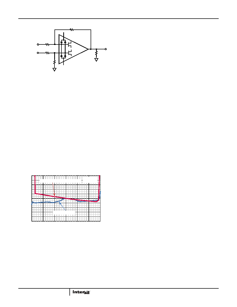
FIGURE 43. INPUT ESD DIODE CURRENT LIMITING
-
+
RIN-
RL
VIN-
V+
V-
RIN+
VIN+
FIGURE 44. INPUT OFFSET VOLTAGE AND BIAS CURRENT vs
COMMON MODE INPUT VOLTAGE
VCM (V)
N
O
R
M
A
L
IZ
E
D
IN
P
U
T
B
IA
S
C
U
R
E
N
T
(p
A
)
-10
-8
-6
-4
-2
0
2
4
6
8
10
-15
-10
-5
0
5
10
15
-500
-400
-300
-200
-100
0
100
200
300
400
500
N
O
R
M
A
L
IZ
E
D
V
O
S
(u
V
)
VS = ±15V
T = +25°C
INPUT OFFSET VOLTAGE (VOS)
INPUT BIAS (IB)
相关PDF资料 |
PDF描述 |
|---|---|
| 160666-4 | CONN UNINS RECPT 22-26AWG 0.110 |
| N3627-6603 | CONN HEADER 24POS STR LONG LATCH |
| 929665-01-25-EU | CONN HEADER 50POS .100 DUAL STR |
| 961130-5900-AR-PT | CONN HEADER R/A 30POS GOLD SMD |
| 961242-6300-AR-TP | CONN HEADER STR DL 42PS GOLD SMD |
相关代理商/技术参数 |
参数描述 |
|---|---|
| ISL28110FBZ-T7 | 功能描述:放大器 IC 开发工具 ISL28110FBZ SINGLE PRECISION LW NOISE RoHS:否 制造商:International Rectifier 产品:Demonstration Boards 类型:Power Amplifiers 工具用于评估:IR4302 工作电源电压:13 V to 23 V |
| ISL28110FBZ-T7A | 功能描述:放大器 IC 开发工具 ISL28110FBZ SINGLE PRECISION LW NOISE RoHS:否 制造商:International Rectifier 产品:Demonstration Boards 类型:Power Amplifiers 工具用于评估:IR4302 工作电源电压:13 V to 23 V |
| ISL28110FRTBZ | 制造商:INTERSIL 制造商全称:Intersil Corporation 功能描述:Precision Low Noise JFET Operational Amplifiers |
| ISL28110FRTZ | 制造商:INTERSIL 制造商全称:Intersil Corporation 功能描述:Precision Low Noise JFET Operational Amplifiers |
| ISL28110FUBZ | 制造商:INTERSIL 制造商全称:Intersil Corporation 功能描述:Precision Low Noise JFET Operational Amplifiers |
发布紧急采购,3分钟左右您将得到回复。