- 您现在的位置:买卖IC网 > PDF目录20678 > ISL28118MUZ (Intersil)IC OPAMP PREC R-R 4MHZ LP 8MSOP PDF资料下载
参数资料
| 型号: | ISL28118MUZ |
| 厂商: | Intersil |
| 文件页数: | 18/23页 |
| 文件大小: | 0K |
| 描述: | IC OPAMP PREC R-R 4MHZ LP 8MSOP |
| 标准包装: | 50 |
| 放大器类型: | 通用 |
| 电路数: | 1 |
| 输出类型: | 满摆幅 |
| 转换速率: | 1.2 V/µs |
| 增益带宽积: | 4MHz |
| 电流 - 输入偏压: | 230nA |
| 电压 - 输入偏移: | 25µV |
| 电流 - 电源: | 850µA |
| 电流 - 输出 / 通道: | 28mA |
| 电压 - 电源,单路/双路(±): | 3 V ~ 40 V,-1.2 V/+1.8 V ~ ±20 V |
| 工作温度: | -55°C ~ 125°C |
| 安装类型: | * |
| 封装/外壳: | * |
| 供应商设备封装: | * |
| 包装: | * |
ISL28118M
4
FN7858.1
March 7, 2014
Absolute Maximum Ratings
Thermal Information
Maximum Supply Voltage . . . . . . . . . . . . . . . . . . . . . . . . . . . . . . . . . . . . . 42V
Maximum Differential Input Current . . . . . . . . . . . . . . . . . . . . . . . . . . 20mA
Maximum Differential Input Voltage . . . . . . . .42V or V- - 0.5V to V+ + 0.5V
Min/Max Input Voltage . . . . . . . . . . . . . . . . . . .42V or V- - 0.5V to V+ + 0.5V
Max/Min Input Current . . . . . . . . . . . . . . . . . . . . . . . . . . . . . . . . . . . . . . . . . . ±20mA
Output Short-Circuit Duration (1 output at a time) . . . . . . . . . . . . . . Indefinite
ESD Tolerance
Human Body Model (Tested per JESD22-A114F) . . . . . . . . . . . . . . . . 3kV
Machine Model (Tested per JESD22-A115-A) . . . . . . . . . . . . . . . . . . 300V
Charged Device Model (Tested per CDM-22CI0ID). . . . . . . . . . . . . . . 2kV
Thermal Resistance (Typical)
θJA (°C/W)
θJC (°C/W)
8 Ld MSOP Package (Notes 4, 5) . . . . . . . . .
165
57
Storage Temperature Range. . . . . . . . . . . . . . . . . . . . . . . .-65°C to +150°C
Pb-free Reflow Profile . . . . . . . . . . . . . . . . . . . . . . . . . . . . . . . see link below
Operating Conditions
Ambient Operating Temperature Range . . . . . . . . . . . . . .-55°C to +125°C
Maximum Operating Junction Temperature . . . . . . . . . . . . . . . . . .+150°C
Supply Voltage . . . . . . . . . . . . . . . . . . . . . . 3V (+1.8V/-1.2V) to 40V (±20V)
CAUTION: Do not operate at or near the maximum ratings listed for extended periods of time. Exposure to such conditions may adversely impact product
reliability and result in failures not covered by warranty.
NOTES:
4.
θJA is measured with the component mounted on a high effective thermal conductivity test board in free air. See Tech Brief TB379 for details.
5. For
θJC, the “case temp” location is taken at the package top center.
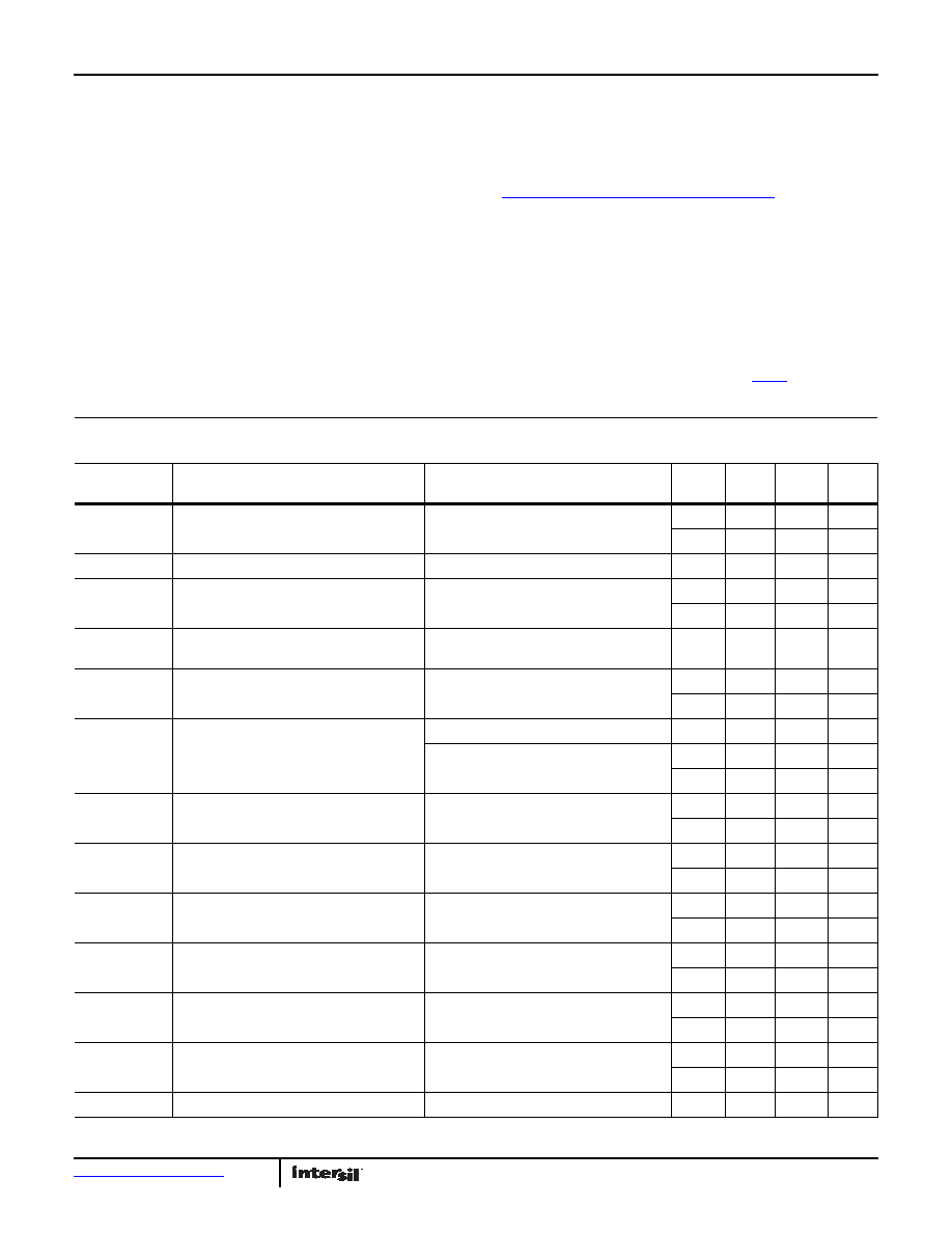
Electrical Specifications, VS ±15 VCM= 0, VO= 0V, RL = Open, TA= +25°C, unless otherwise noted. Boldface limits apply across the
operating temperature range, -55°C to +125°C. Temperature data established by characterization.
PARAMETER
DESCRIPTION
CONDITIONS
MIN
(Note 6)
TYP
MAX
(Note 6)
UNIT
VOS
Input Offset Voltage
-150
25
150
V
-270
270
V
TCVOS
Input Offset Voltage Temperature Coefficient
-1.2
0.2
1.2
V/°C
IB
Input Bias Current
-575
-230
nA
-800
nA
TCIB
Input Bias Current
Temperature Coefficient
-0.8
nA/°C
IOS
Input Offset Current
-50
4
50
nA
-75
75
nA
CMRR
Common-Mode Rejection Ratio
VCM = V- - 0.5V to V+ - 1.8V
118
dB
VCM = V- to V+ -1.8V
102
118
dB
97
dB
VCMIR
Common Mode Input Voltage Range
Guaranteed by CMRR test
V- - 0.5
V+ - 1.8
V
V-
V+ - 1.8
V
PSRR
Power Supply Rejection Ratio
VS = 3V to 40V, VCMIR = Valid Input Voltage
109
124
dB
105
dB
AVOL
Open-Loop Gain
VO = -13V to +13V, RL = 10kΩ to ground
120
136
dB
114
dB
VOL
Output Voltage Low,
VOUT to V-
RL = 10kΩ
70
mV
85
mV
VOH
Output Voltage High,
V+ to VOUT
RL = 10kΩ
110
mV
120
mV
IS
Supply Current/Amplifier
RL = Open
0.85
1.2
mA
1.6
mA
ISC+
Output Short Circuit Source Current
RL = 10Ω to V-
16
mA
相关PDF资料 |
PDF描述 |
|---|---|
| S1PD-M3/84A | DIODE GPP 1A 200V SMP |
| GCM12DRTI | CONN EDGECARD 24POS DIP .156 SLD |
| AISC-0805-R012J-T | INDUCTOR WW CERAM 12.0NH 0805 |
| VE-2NK-CX | CONVERTER MOD DC/DC 40V 75W |
| ISL8112IRZ | IC REG DL BCK/LINEAR SYNC 32-QFN |
相关代理商/技术参数 |
参数描述 |
|---|---|
| ISL28118MUZ-T13 | 功能描述:放大器 IC 开发工具 ISL28118MUZ 40V LW NOIS R-R OT SNGL SUP RoHS:否 制造商:International Rectifier 产品:Demonstration Boards 类型:Power Amplifiers 工具用于评估:IR4302 工作电源电压:13 V to 23 V |
| ISL28118MUZ-T7 | 功能描述:放大器 IC 开发工具 ISL28118MUZ 40V LW NOIS R-R OT SNGL SUP RoHS:否 制造商:International Rectifier 产品:Demonstration Boards 类型:Power Amplifiers 工具用于评估:IR4302 工作电源电压:13 V to 23 V |
| ISL28118MUZ-T7A | 功能描述:精密放大器 ISL28118MUZ 40V LW NOISE RAIL-RAIL OUT RoHS:否 制造商:Maxim Integrated 每芯片的通道数量: 输入补偿电压:0.25 mV at +/- 5 V 输入电压范围(最大值): 安装风格: 封装 / 箱体:SOIC-8 Narrow 封装:Tube |
| ISL28127 | 制造商:INTERSIL 制造商全称:Intersil Corporation 功能描述:Precision Single and Dual Low Noise Operational Amplifiers |
| ISL28127_10 | 制造商:INTERSIL 制造商全称:Intersil Corporation 功能描述:Precision Single and Dual Low Noise Operational Amplifiers |
发布紧急采购,3分钟左右您将得到回复。